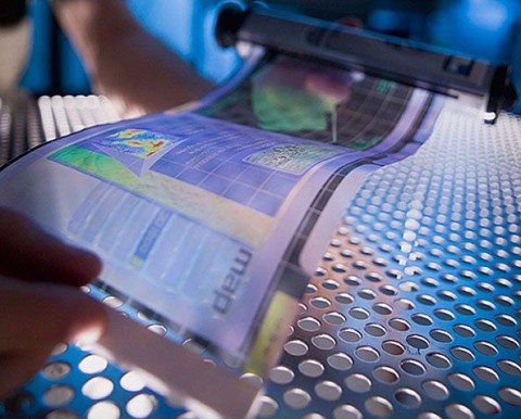
HP and Arizona State University have demonstrated what they’re calling the first prototype of “affordable, flexible electronic displays”. Constructed using the self-aligned imprint lithography (SAIL) technology invented by HP Labs, the display also uses E Ink’s Vizplex bi-stable electrophoretic imaging film that requires no power to maintain an image; the end result is a low-power, low-manufacturing-cost display suitable for color text and graphics.

Rather than being produced in sheets, in a batch process, SAIL allows the different layers to be combined in a roll-to-roll process. That continuous build reduces manufacturing complexity and material usage (up to 90-percent less materials by volume, in fact) and thus cost. It’s also being called “unbreakable”, with the patterning information imprinted in such a way that distortion does not impact perfect alignment.
HP envisage the new display technology to be used in laptops, smartphones and other electronic devices. Not only will form factors be able to change, thanks to the flexible screen, but the could be cheaper, too.
Press Release:
HP and Arizona State University Demo Flexible, Unbreakable Displays
Summary - HP and the Flexible Display Center (FDC) at Arizona State University (ASU) today announced the first prototype of affordable, flexible electronic displays.
Flexible displays are paper-like computer displays made almost entirely of plastic. This technology enables displays to become easily portable and consumes less power than today’s computer displays. Popular applications for the technology could include electronic paper and signage.
The production feat is a milestone in the industry’s efforts to create a mass market for high-resolution flexible displays. Plus, from an environmental standpoint, the displays leapfrog conventional display processes by using up to 90 percent less materials by volume.
Mass production of such displays can enable production of notebook computers, smart phones and other electronic devices at much lower costs since the display is one of the more costly components.
The unbreakable displays were created by the FDC and HP using self-aligned imprint lithography (SAIL) technology invented in HP Labs, HP’s central research arm. SAIL is considered “self aligned” because the patterning information is imprinted on the substrate in such a way that perfect alignment is maintained regardless of process-induced distortion.
SAIL technology enables the fabrication of thin film transistor arrays on a flexible plastic material in a low-cost, roll-to-roll manufacturing process. This allows for more cost-effective continuous production, rather than batch sheet-to-sheet production.
“The display HP has created with the FDC proves the technology and demonstrates the remarkable innovation we’re bringing to the rapidly growing display market,” said Carl Taussig, director, Information Surfaces, HP Labs. “In addition to providing a lower-cost process, SAIL technology represents a more sustainable, environmentally sensitive approach to producing electronic displays.”
Production of flexible displays
The first practical demonstration of the flexible displays was achieved through collaborative efforts between the FDC and HP as well as other FDC partners including DuPont Teijin Films and E Ink. To create this display, the FDC produces stacks of semiconductor materials and metals on flexible Teonex® Polyethylene Naphthalate (PEN) substrates from DuPont Teijin Films.
HP then patterns the substrates using the SAIL process and subsequently integrates E Ink’s Vizplex™ imaging film to produce an actively addressed flexible display on plastic. E Ink’s Vizplex bi-stable electrophoretic imaging film enables images to persist without applied voltage, thereby greatly reducing power consumption for viewing text.
“Producing a photolithography-free, flexible active-matrix display is an excellent example of the Flexible Display Center’s world-class development and manufacturing infrastructure,” said Shawn O’Rourke, director, Engineering, Flexible Display Center at Arizona State University. “It demonstrates how multiple industry partners can collaborate on innovative solutions, including roll-to-roll compatible technology that addresses the rapidly growing market for flexible electronics.”
“Flexible electronic displays are playing an increasingly important role in the global high-tech industry, serving as the crucial enabling technology for a new generation of portable devices, including e-readers and similar products designed to combine mobility with compelling user interfaces,” said Vinita Jakhanwal, principal analyst, Small and Medium Displays, iSuppli. “We expect the flexible display market to grow from $80 million in 2007 to $2.8 billion by 2013. The Flexible Display Center at Arizona State University is a key participant in helping to develop the technology and manufacturing ecosystem to support this market.”
HP SAIL technology is one example of the technologies available for licensing from the HP Intellectual Property Licensing Group.
Further information about DuPont Teijin Films is available at www.dupontteijinfilms.com.
About ASU Flexible Display Center
The FDC is a government–industry–academia partnership that’s advancing full-color flexible display technology and fostering development of a manufacturing ecosystem to support the rapidly growing market for flexible electronic displays. FDC partners include many of the world’s leading providers of advanced display technology, materials and process equipment. The FDC is unique among the U.S. Army’s University centers, having been formed through a 10-year cooperative agreement with Arizona State University in 2004. This adaptable agreement has enabled the FDC to create and implement a proven collaborative partnership model with more than 20 engaged industry members, and to successfully deploy world-class wafer-scale R&D and GEN-II display-scale pilot production lines for rapid flexible display technology development and manufacturing supply chain commercialization. More information about FDC is available at http://flexdisplay.asu.edu/.
About HP
HP, the world’s largest technology company, simplifies the technology experience for consumers and businesses with a portfolio that spans printing, personal computing, software, services and IT infrastructure. More information about HP (NYSE: HPQ) is available at http://www.hp.com/.


