Showing posts with label data storage. Show all posts

Thursday, June 4, 2009

A billion year ultra-dense nanotechnology memory chip

Posted: June 4, 2009

(Nanowerk News) When it comes to data storage, density and durability have always moved in opposite directions - the greater the density the shorter the durability. For example, information carved in stone is not dense but can last thousands of years, whereas today’s silicon memory chips can hold their information for only a few decades. Researchers with the U.S. Department of Energy’s Lawrence Berkeley National Laboratory (Berkeley Lab) and the University of California (UC) Berkeley have smashed this tradition with a new memory storage medium that can pack thousands of times more data into one square inch of space than conventional chips and preserve this data for more than a billion years!
This video shows an iron nanoparticle shuttle moving through a carbon nanotube in the presence of a low voltage electrical current. The shuttle’s position inside the tube can function as a high-density nonvolatile memory element. (Courtesy of Zettl Research Group)
“We’ve developed a new mechanism for digital memory storage that consists of a crystalline iron nanoparticle shuttle enclosed within the hollow of a multiwalled carbon nanotube,” said physicist Alex Zettl who led this research.
“Through this combination of nanomaterials and interactions, we’ve created a memory device that features both ultra-high density and ultra-long lifetimes, and that can be written to and read from using the conventional voltages already available in digital electronics.”
Zettl, one of the world’s foremost researchers into nanoscale systems and devices, holds joint appointments with Berkeley Lab’s Materials Sciences Division (MSD) and the Physics Department at UC Berkeley, where he is the director of the Center of Integrated Nanomechanical Systems. He is the principal author of a paper that has been published on-line by Nano Letters entitled: “Nanoscale Reversible Mass Transport for Archival Memory.” Co-authoring the paper with Zettl were Gavi Begtrup, Will Gannett and Tom Yuzvinsky, all members of his research group, plus Vincent Crespi, a theorist at Penn State University.
The ever-growing demand for digital storage of videos, images, music and text calls for storage media that pack increasingly more data onto chips that keep shrinking in size. However, this demand runs in sharp contrast to the history of data storage. Compare the stone carvings in the Egyptian temple of Karnak, which store approximately two bits of data per square inch but can still be read after nearly 4,000 years, to a modern DVD which can store 100 giga (billion) bits of data per square inch but will probably remain readable for no more than 30 years.
“Interestingly,” said Zettl, “the Domesday Book, the great survey of England commissioned by William the Conqueror in 1086 and written on vellum, has survived over 900 years, while the 1986 BBC Domesday Project, a multimedia survey marking the 900th anniversary of the original Book, required migration from the original high-density laserdiscs within two decades because of media failure.”
Zettl and his collaborators were able to buck data storage history by creating a programmable memory system that is based on a moveable part - an iron nanoparticle, approximately 1/50,000th the width of a human hair, that in the presence of a low voltage electrical current can be shuttled back and forth inside a hollow carbon nanotube with remarkable precision. The shuttle’s position inside the tube can be read out directly via a simple measurement of electrical resistance, allowing the shuttle to function as a nonvolatile memory element with potentially hundreds of binary memory states.
“The shuttle memory has application for archival data storage with information density as high as one trillion bits per square inch and thermodynamic stability in excess of one billion years,” Zettl said. “Furthermore, as the system is naturally hermetically sealed, it provides its own protection against environmental contamination.”
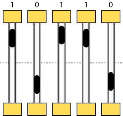
The nanoscale electromechanical memory device can write/read data based on the position of an iron nanoparticle in a carbon nanotube
The nanoscale electromechanical memory device can write/read data based on the position of an iron nanoparticle in a carbon nanotube. In this schematic, the memory devices are displaying a binary sequence 1 0 1 1 0 (Image: Zettl Research Group, Lawrence Berkeley National Laboratory and University of California at Berkeley.)
The low voltage electrical write/read capabilities of the memory element in this electromechanical device facilitates large-scale integration and should make for easy incorporation into today’s silicon processing systems. Zettl believes the technology could be on the market within the next two years and its impact should be significant.
“Although truly archival storage is a global property of an entire memory system, the first requirement is that the underlying mechanism of information storage for individual bits must exhibit a persistence time much longer than the envisioned lifetime of the resulting device,” he said. “A single bit lifetime in excess of a billion years demonstrates that our system has the potential to store information reliably for any practical desired archival time scale.”
The multiwalled carbon nanotube and enclosed iron nanoparticle shuttle were synthesized in a single step via pyrolysis of ferrocene in argon gas at a temperature of 1,000 degrees Celsius. The nanotube memory elements were then ultrasonically dispersed in isopropanol and deposited on a substrate. A transmission electron microscope provided high-resolution imaging in real time while the memory device was in operation. In laboratory tests, this device met all the essential requirements for digital memory storage including the ability to overwrite old data.
“We believe our nanoscale electromechanical memory system presents a new solution to the challenge of ultra-high density archival data storage,” Zettl said.
Source: Berkeley Lab

Source

Tuesday, December 9, 2008

Nano-magnetic sensors could pave the way for massive data storage capacity

Trendwatch
By Rick C. Hodgin
Tuesday, December 09, 2008 14:25

Troy (NY) - Researchers at Rensselaer Polytechnic Institute (RPI) have created nanoscopic magnetic sensors. Comprised of carbon nanotubes embedded with bundles of cobalt atoms, these magnetic field sensors are the first ever capable of reliably detecting magnetic fields at near atomic levels.

RPI is calling its discovery "a new class of magnetic materials." The nano-device's cobalt clusters are embedded within the walls of a multi-layered carbon nanotube, just 1 nm to 10 nm in diameter. Since the clusters are internal to the tubes, rather than external, "they do not cause electron scattering and thus do not seem to impact the attractive conductive properties of the host carbon nanotube," according to assistant professor Swastik Kar, Department of Physics, who led the project.

A series of experiments has shown that the cobalt-cluster carbon nanotubes are sensitive enough to detect even miniscule magnetic fields present at near-atomic levels. RPI believes this is the first time such small magnetic fields have been reliably detected using carbon nanotubes, and it provides a new tool for analyzing the nanoscopic magnetic properties of many everyday items - something that was not possible previously due to an interference of the source materials used in the detector.


Future applications

According to the research paper, potential future applications include "new generations of nanoscale conductance sensors, new advances in digital storage devices, spintronics, and selective drug delivery components." Today's most advanced perpendicular storage techniques allow up to around 200 Gb of data per square inch (25 Gigabytes). Hard drives on the order of 10 nm per bit would allow upwards of 10 Petabits (Pb) per square inch - though realistic applications would be closer to 100 Terabits per square inch. Perpendicular storage solutions are expected to max out around 1 Terabit per square inch, though this ceiling appears to be constantly moving.

Today, semiconductors companies often utilize infrared emissions to detect electron movement through silicon-based transistors. TG Daily had the opportunity to visit Intel's debug lab in Nov, 2007. The laser probes used in that lab detect the emission of infrared light, which is transparent to silicon, and seeps through the back of the chip while the CPU is running.

By monitoring photon activity on the chip with the laser probe, the CPU debuggers can isolate individual circuits in operation. This helps them detect errors for chip designers and track down other problems or inefficiencies. This new RPI device may also produce an alternate method for detecting this kind of circuit activity.

The results of this study were published in an article entitled "Detection of Nanoscale Magnetic Activity Using a Single Carbon Nanotube" in Nano Letters.


Funding

Funding for this project was provided by the New York State Interconnect Focus Center at Rensselaer. Additional authors on the Nano Letters paper include Caterina Soldano, a postdoctoral research assistant at the Centre d’Elaboration de Matériaux et d’Etudes Structurales in Tolouse, France. Also, Professor Saikat Talapatra of the Physics Department of Southern Illinois University-Carbondale. And Professor P.M. Ajayan of Rice University's Department of Mechanical Engineering and Materials Science.


Other research

Additional recent carbon nanotube-related research from RPI includes a nanoscopic pressure sensor made of carbon nanotubes. RPI has also recently developed a solar cell coating which allows panels to absorb 90% of sunlight without the need for servos which track the sun's movement across the sky.

Source

Tuesday, May 27, 2008

HEWLETT-PACKARD CNT Memory Data Storage

Data storage device including nanotube electron sources
HEWLETT-PACKARD
Priority date July 6, 2001


United States Patent Application 20030007443
Kind Code A1
Nickel, Janice H. January 9, 2003


Matured to USP 6,928,042

What is claimed is:
1. A data storage device comprising an array of nanotubes as electron sources; and a phase-change storage layer proximate tips of the electron sources.

And USP 7,295,503

What is claimed is:

1. A data storage device comprising an array of nanotubes as electron sources.

2. The device of claim 1, wherein the nanotubes are carbon-based.


3. The device of claim 1, wherein the nanotubes are boron nitride-based.

4. The device of claim 1, further comprising a phase-change storage layer proximate tips of the electron sources.

5. The device of claim 1, wherein each nanotube electron source is elongated.

6. The device of claim 5, wherein the nanotubes have an aspect ratio greater than 10:1.

7. The device of claim 1, further comprising word and bit lines for addressing the nanotubes.

8. The device of claim 1, further comprising a micromover for positioning the array.

9. A data storage device comprising: an array of carbon-based nanotubes; and a phase-change storage layer proximate tips of the nanotubes.

10. A data storage device comprising: an array of boron nitride-based nanotubes; and a phase-change storage layer proximate tips of the nanotubes.

11. An electron beam source for a data storage device, the source comprising an array of nanotubes.

12. The electron beam source of claim 11, wherein the nanotubes are carbon nanotubes.


13. The electron beam source of claim 11, wherein the nanotubes are boron nitride nanotubes.

14. The source of claim 11, wherein the nanotubes have an aspect ratio greater than 10:1.

15. The source of claim 11, further comprising word and bit lines for addressing the nanotubes.

16. The device of claim 11, further comprising a micromover for positioning the array.
--------------------------------------------------------------------------------

Description

--------------------------------------------------------------------------------


BACKGROUND

[0001] The present invention relates generally to electron sources. The present invention also relates to data storage devices.

[0002] For decades researchers have been working to increase storage density and reduce storage cost of data storage devices such as magnetic hard-drives, optical drives, and semiconductor random access memory. However, increasing the storage density is becoming increasingly difficult because conventional technologies appear to be approaching fundamental limits on storage density. For instance, information storage based on conventional magnetic recording is rapidly approaching fundamental physical limits such as the superparamagnetic limit, below which magnetic bits are not stable at room temperature.

[0003] Storage devices that do not face these fundamental limits are being researched. An example of such an information storage device is described in Gibson et al. U.S. Pat. No. 5,557,596. The device includes multiple electron sources having electron emission surfaces that are proximate a storage medium. During write operations, the electron sources bombard the storage medium with relatively high intensity electron beams. During read operations, the electron sources bombard the storage medium with relatively low intensity electron beams.

[0004] Size of storage bits in such a device may be reduced by decreasing the electron beam diameter. Reducing the storage bit size increases storage density and capacity, and it decreases storage cost.

[0005] "Spindt" emitters could be used for generating focused electron beams in such a device. A Spindt emitter has a conical shape and emits an electron beam at the tip of its cone. The cone tip is made as sharp as possible to reduce operating voltage and achieve a small electron beam diameter.

[0006] However, certain problems arise with Spindt emitters. One problem is that the Spindt emitters are sensitive to impact. The tips of the Spindt emitters are only a few nanometers from the storage medium. If a tip makes contact with the storage medium, it could be damaged. Another problem is directionality of the electron beams emitted from the Spindt emitters. Sometimes an electron beam can come off the side of the cone rather than the tip. Yet another problem is a loss of material from the tips due to energy being greater than the workfunction. The loss of material reduces the effectiveness of the tips.

SUMMARY

[0007] According to one aspect of the present invention, a data storage device includes nanotubes as electron sources. Other aspects and advantages of the present invention will become apparent from the following detailed description, taken in conjunction with the accompanying drawings, illustrating by way of example the principles of the present invention.

LINK

This filing looks like the dominant one - earliest priority date - July 6, 2001.

These are all noted here:
http://www.geocities.com/mr_module/NanoDataRecorders.html?1094841052781