Showing posts with label graphene. Show all posts

Wednesday, March 3, 2010

Helping Hydrogen: Student Inventor Tackles Challenge of Hydrogen Storage


Listen to a podcast interview with Lemelson-MIT Rensselaer Student Prize-Winner Javad Rafiee.

$30,000 Lemelson-MIT Collegiate Student Prizes Awarded to Inventive Students Nationwide; Four Leading Institutes Celebrate 2010 Winners

Determined to play a key role in solving global dependency on fossil fuels, Javad Rafiee, a doctoral student in the Department of Mechanical, Aerospace, and Nuclear Engineering at Rensselaer Polytechnic Institute, has developed a new method for storing hydrogen at room temperature.

Rafiee has created a novel form of engineered graphene that exhibits hydrogen storing capacity far exceeding any other known material. For this innovation, which brings the world a step closer to realizing the widespread adoption of clean, abundant hydrogen as a fuel for transportation vehicles, Rafiee is the winner of the 2010 $30,000 Lemelson-MIT Rensselaer Student Prize. He is among the four 2010 $30,000 Lemelson-MIT Collegiate Student Prize winners announced today.

“Invention is the key ingredient of progress, and the Lemelson-MIT Rensselaer Student Prize rallies our students to innovate world-changing solutions for the grand challenges facing all people of all nations,” said Rensselaer President Shirley Ann Jackson. “Javad Rafiee has the vision of a robust national hydrogen economy and a world less dependent on oil and gasoline. I applaud his efforts toward this noble goal, and congratulate him on this prestigious award. I thank all of the Lemelson-MIT Rensselaer Collegiate Student Prize winners and finalists for their effort, zeal, and for being ambassadors of progress.”

Rafiee is the fourth recipient of the Lemelson-MIT Rensselaer Student Prize. The prize, first given in 2007, is awarded annually to a Rensselaer senior or graduate student who has created or improved a product or process, applied a technology in a new way, redesigned a system, or demonstrated remarkable inventiveness in other ways.

"This year’s winners from the Massachusetts Institute of Technology, California Institute of Technology, Rensselaer Polytechnic Institute, and University of Illinois at Urbana-Champaign shine light on the significance of collegiate invention. They have the ability to transform seemingly implausible ideas into reality and are the true entrepreneurial leaders of their generation,” said Joshua Schuler, executive director of the Lemelson-MIT Program.

For videos and photos of the winner and award finalists, as well as a Webcast of the announcement ceremony, please visit: www.eng.rpi.edu/lemelson.

Enabling Greener Transportation with Graphene
Hydrogen storage has proven to be a significant bottleneck to the advancement and proliferation of fuel cell and hydrogen technologies in cars, trucks, and other applications. Rafiee has developed a new method for manufacturing and using graphene, an atom-thick sheet of carbon atoms arranged like a nanoscale chain-link fence, to store hydrogen. His solution is inexpensive and easy to produce.

With adviser and Rensselaer Professor Nikhil Koratkar, Rafiee used a combination of mechanical grinding, plasma treatment, and annealing to engineer the atomic structure of graphene to maximize its hydrogen storage capacity. This new graphene has exhibited a hydrogen storage capacity of 14 percent by weight at room temperature – far exceeding any other known material.

This 14-percent capacity surpasses the U.S. Department of Energy 2015 target of realizing a material with hydrogen storage capacity of 9 percent by weight at room temperature. Rafiee said his graphene is also one of the first known materials to surpass the Department of Energy’s 2010 target of 6 percent.

Rafiee’s graphene exhibits three critical attributes that result in its unique hydrogen storage capacity. The first is high surface area. Graphene’s unique structure, only one atom thick, means that each of its carbon atoms is exposed to the environment and, in turn, to the hydrogen gas. The second attribute is low density. Graphene has one of the highest surface area-per-unit masses in nature, far superior to even carbon nanotubes and fullerenes.

The third attribute is favorable surface chemistry. After oxidizing graphite powder and mechanically grinding the resulting graphite oxide, Rafiee synthesized the graphene by thermal shock followed by annealing and exposure to argon plasma. These treatments play an important role in increasing the binding energy of hydrogen to the graphene surface at room temperature, as hydrogen tends to cluster and layer around carbon atoms.

Talented Engineer
Rafiee joined Rensselaer in 2008, following an internship at the City University of Hong Kong and earning his bachelor’s and master’s degrees in mechanical and manufacturing engineering from the University of Tabriz in Iran. At Rensselaer, Rafiee and his brother, Mohammad, joined the research group of Mechanical, Aerospace, and Nuclear Engineering Professor Nikhil Koratkar.

“Javad is extremely knowledgeable, has great confidence in his abilities, and has demonstrated a very high level of creativity and originality. However, it is his deep passion and enthusiasm for research and discovery coupled with his amazing drive and energy that differentiates him from his peers,” Koratkar said. “This passion and excitement for discovery and innovation is not something that can be taught or learned. It is an intrinsic quality of an individual – either you have it or you don’t — and Javad is the most intellectually curious student I have ever had the privilege to advise here at Rensselaer.”

In his time at Rensselaer, Rafiee has authored five, and co-authored three, journal papers in various disciplines, ranging from materials science and mechanical engineering, to computer science and urology.

Rafiee is from Tehran, Iran, and expects to earn his doctorate in 2011. Following graduation, he and his brother plan to start their own business with a focus on clean energy and green manufacturing.

Source

Saturday, October 31, 2009

Closest Look Ever at Graphene

10/31/2009 2:15:29 AM
Closest Look Ever at Graphene: Stunning Images of Individual Carbon Atoms From TEAM 0.5 microscope


Source

Thursday, February 5, 2009

Graphene for the Green Grid

Thursday, February 05, 2009

Ultracapacitors that store more could help the grid run smoothly.

By Katherine Bourzac

Graphene power: Graphene Energy hopes that graphene electrodes such as this one will increase the energy-storage capacity and power output of ultracapacitors. This image, which shows the edge of a graphene electrode, was made with a scanning-electron microscope.
Credit: Meryl Stoller

Integrating irregular sources of renewable energy, such as wind and solar, with the electrical grid, while keeping power output steady, is going to be a big challenge. Energy-storage devices called ultracapacitors could help by storing sudden surges of power. But much will depend on developing a new generation of ultracapacitors with enough storage capacity to meet the likely demand.

Graphene Energy, a startup based in Austin, TX, hopes that ultracapacitors with electrodes made of graphene--sheets of carbon just an atom thick--will be the solution. The storage capacity of an ultracapacitor is limited only by the surface area of its electrodes, and graphene offers a way to greatly increase the area available.

Ultracapacitors store energy electrostatically, instead of chemically, as in batteries. During charging, electrons come to the surface of one electrode, and electron "holes" form on the surface of the other. This draws positive ions in an electrolyte to the first electrode and negative ions to the second. By contrast, the chemical reactions used to charge batteries limit the speed with which they can be charged and eventually cause the electrode materials to break down. Ultracapacitors can be charged and discharged very rapidly, in seconds rather than minutes, and can be recharged millions of times before wearing out.

However, ultracapacitors currently on the market can't match batteries for energy density, so they're mostly used in hybrid systems alongside batteries or for niche applications. Because these devices can handle a rapid influx of large amounts of energy, they're often used to recover energy--for example, when a city bus breaks or a gantry crane lowers its cargo. Ultracapacitors employed in this way have reduced by 40 percent the energy needed by some cranes used in Japanese ports. A few power tools, including an electric drill, take advantage of the rapid recharging ability of ultracapacitors.

Graphene Energy hopes to open up new ultracapacitor applications by developing devices with far higher power output. These ultracapacitors could perhaps be used to regulate surges in the electrical grid or to power hybrid transportation vehicles. The company has $500,000 in seed funding to commercialize graphene ultracapacitors developed by Rodney Ruoff, a professor and chair of mechanical engineering at the University of Texas at Austin. Ruoff is a cofounder of Graphene Energy and also serves as the company's technology advisor.

Existing ultracapacitors use electrodes made from activated carbon--a porous, charcoal-like material that has a very high surface area. Activated carbon stores charge in tunnel-like pores, and it takes about one second for it to travel in and out. This is very fast compared with the fastest batteries, but activated carbon has a limited power output.

To make the graphene for its electrodes, Ruoff's team starts by putting graphite oxide in a water solution. This causes the material to flake into atom-thin sheets of graphene oxide. Next, the oxygen atoms are removed, leaving the graphene behind. So far, Ruoff's lab has made graphene ultracapacitors that match the performance of those made using activated carbon. With further refinements, he says, they should outperform activated carbon, although the steps that his company is taking to achieve this remain secret.

Based on a description of the graphene ultracapacitors published last September in the journal Nano Letters, John Miller of JME, a research and consulting firm that specializes in electrochemical capacitors, says that it should indeed be possible to improve their performance. The graphene electrode described in this paper is "wadded into a ball like a crumpled piece of paper," says Miller. "You don't have full access to the surface."

If Graphene Energy can grow the electrodes in vertical arrays, like a row of perfectly flat sheets of paper standing on edge, Miller says that the power output could be increased dramatically. In this arrangement, every single carbon atom would be exposed and able to store energy, with virtually no waiting time for the charge to travel down the tunnels found in activated carbon.

However, in addition to improving the performance of its ultracapacitors, Graphene Energy must also develop a method for making them at larger scales--a common challenge across all graphene research.

Dileep Agnihotri, CEO of Graphene Energy, says that the company hopes to test its first prototype product incorporating graphene electrodes by the end of this year.

Another group of researchers hopes to make better ultracapacitor electrodes using carbon nanotubes--rolled-up tubes of graphene that have many of the same properties. "I think both approaches can work in principle," says Joel Schindall, a professor of electrical engineering and computer science at MIT who is working on the nanotube electrodes. "The key will be getting the growth process right, then working on ways to manufacture it in a cost-effective manner."

http://www.technologyreview.com/business/22062/?nlid=1752&a=f

Tuesday, October 28, 2008

Graphene could accelerate genomics

Oct 28, 2008
DNA moving through a graphene nanogap

Artist's impression of a DNA molecule (helix) moving through a tiny slit in a graphene sheet (shown in blue). (Courtesy: Henk Postma)

The “wonder material” graphene could soon be used to analyse DNA at a record-breaking pace. That’s the claim of a physicist in the US who has proposed a new way of reading the sequence of chemical bases in a DNA strand by sending the molecule through a tiny slit in a graphene sheet.

While the technique has yet to be verified experimentally, if successful it could be eligible for the $10 million X Prize for Genomics, which has set the challenge of developing a new rapid and low-cost sequencing technology.

The genetic profile — or “genome” — of an organism is determined by recording the full sequence of acid base pairs that make up its DNA. In 2003, the Human Genome Project made history by determining the entire human genetic code — 3 billion DNA base pairs that took 13 years to analyse using a technique that has changed very little since the late 1970s.

This “shotgun” approach first isolates a DNA strand and forces it to copy itself millions of times over in a chemical reaction. These are then “blasted” into tiny fragments because current techniques for sequence reading can detectors can only analyse very short sections of DNA. Finally, a supercomputer matches up overlapping base patterns to piece together the full genome.

No processing required

Now, Henk Postma at California State University Northridge has proposed a way of sequencing an entire DNA strand without the need for blasting or computer processing (arXiv:0810.3035v1 ).

Rapid Sequencing of Individual DNA Molecules in Graphene Nanogaps
http://arxiv.org/PS_cache/arxiv/pdf/0810/0810.3035v1.pdf

The technique involves cutting a very narrow slit or “nanogap” along the length of a piece of graphene — an extremely strong sheet of carbon just one atom thick. A voltage is applied perpendicular to the graphene’s surface, which causes the DNA strand to pass slowly through the slit one base at a time.

A second voltage is applied across slit and electrons are able to “tunnel” across the nanogap via the base that happens to be passing through the slit. There are four different types of base in a DNA molecule, and each should support a different tunnelling current — allowing the base type to be identified.

While the idea of sequencing DNA by sending it through a tiny gap is not new, previous schemes had relied on using separate materials for the membrane and electrodes — and aligning the two materials has proved to be a considerable challenge. Postma’s design gets around this problem by having the graphene function as both membrane and electrode.

Postma believes that detector could be made from a graphene sheet sandwiched between glass plates that are held together by van der Waals forces.

Technology should be possible

According to Changgu Lee, a mechanical engineer at Colombia University, some of the technology to realize Postma’s design may be available already. “Creating the nanogaps in graphene was demonstrated this year using both STM [scanning tunnelling microscopy] and catalytic cutting with metal particles”, he said.

Postma told physicsworld.com that traditional sequencing techniques are limited to determining about 800 base pairs per recording. By contrast, he estimates his design could yield 100,000 bases per recording, and if run continuously it would read the whole human genome in two and a half hours. He also believes that his technique could lead to sequencing devices that are smaller and cheaper than existing systems.

If successful, Postma's system could be a contender for the X Prize for Genomics, which aims to award $10m to the inventor of a device that can sequence 100 human genomes within 10 days or less,to a specified accuracy and costing no more than $10,000 per genome.

Postma said he is continuing to develop his design, but added: “I published the paper to get feedback from the scientific community, in the open, because I believe that will lead to the best possible technology.”

And it seems DNA experts are ready for a new technology. Geoffrey Baldwin, a molecular biologist from Imperial College in the UK said “to truly develop health care we need the profile of 100s of genomes not just the few we have at the moment”. He added “there is now a great opportunity for a new technique to become the standard in base sequencing”.

About the author

James Dacey is a science journalist based in the UK

Source

Strikes me as a DNA computer in the making.

Friday, September 26, 2008

Graphene-stabilized copper nanoparticles as an air-stable substitute for silver and gold in low-cost ink-jet printable electronics

CLICK pic to ENLARGE

Figure 4. Printed copper patterns. (a) Line patterns for electrical
conductivity measurements. The inset shows a homogeneous and
crack-free print surface. (b) Manually cracked pattern for
investigation of the film thickness after five overprints, revealing a
print thickness of 500 nm per print cycle. The magnification inset of
the fracture surface shows the inner structure of the composite film.
(c) Graph showing the decrease of resistance with larger line width
of the pattern (error bars obtained from five samples at each line
width). The mean electrical conductivity was 1.56 ± 0.48 S cm−1.
(d) Light-emitting diodes directly glued onto printed copper lines.
Norman A Luechinger 2008 Nanotechnology doi: 10.1088/0957-4484/19/44/445201


PDF (611 KB) | References


Norman A Luechinger, Evagelos K Athanassiou and Wendelin J Stark1
Institute for Chemical and Bioengineering, Department of Chemistry and Applied Biosciences, ETH Zurich, CH-8093 Zurich, Switzerland
1 Author to whom any correspondence should be addressed
E-mail: wendelin.stark@chem.ethz.ch

Abstract. Metallic copper nanoparticles were synthesized by a bottom-up approach, and in situ coated with protective shells of graphene in order to get a metal nanopowder of high air stability and chemical inertness. Using an amphiphilic surfactant, a water-based copper nanocolloid could be prepared and successfully printed onto a polymer substrate by conventional ink-jet printing using household printers. The dried printed patterns exhibited strong metallic gloss and an electrical conductivity of >1 S cm-1 without the need for a sintering or densification step. This conductivity currently limits use in electronics to low current application or shielding and decorative effects. The high stability of graphene-coated copper nanoparticles makes them economically a most attractive alternative to silver or gold nanocolloids, and will strongly facilitate the industrial use of metal nanocolloids in consumer goods.

Print publication: Issue 44 (5 November 2008)
Received 11 July 2008, in final form 19 August 2008
Published 26 September 2008

Source

Thursday, September 25, 2008

New Graphene-Based Material Clarifies Graphite Oxide Chemistry

September 25, 2008

AUSTIN, Texas — A new "graphene-based" material that helps solve the structure of graphite oxide and could lead to other potential discoveries of the one-atom thick substance called graphene, which has applications in nanoelectronics, energy storage and production, and transportation such as airplanes and cars, has been created by researchers at The University of Texas at Austin.

To get an idea of the nanomaterial graphene, imagine a lightweight material having the strongest chemical bond in nature and, thus, exceptional mechanical properties. In addition it conducts heat better than any other material and has charge carriers moving through it at a significant fraction of the speed of light. Just an atom thick, graphene consists of a "chickenwire" (or honeycomb) bonding arrangement of carbon atoms—also known as a single layer of graphite.

Mechanical Engineering Professor Rod Ruoff and his co-authors have, for the first time, prepared carbon-13 labeled graphite. They did this by first making graphite that had every "normal" carbon atom having the isotope carbon-12, which is magnetically inactive, replaced with carbon-13, which is magnetically active. They then converted that to carbon-13 labeled graphite oxide and used solid-state nuclear magnetic resonance to discern the detailed chemical structure of graphite oxide.

The work by Ruoff's team will appear in the Sept. 26 issue of the journal Science.

"As a result of our work published in Science, it will now be possible for scientists and engineers to create different types of graphene (by using carbon-13 labeled graphene as the starting material and doing further chemistry to it) and to study such graphene-based materials with solid-state nuclear magnetic resonance to obtain their detailed chemical structure," Ruoff says. "This includes situations such as where the graphene is mixed with a polymer and chemically bonded at critical locations to make remarkable polymer matrix composites; or embedded in glass or ceramic materials; or used in nanoelectronic components; or mixed with an electrolyte to provide superior supercapacitor or battery performance. If we don't know the chemistry in detail, we won't be able to optimize properties."

Graphene-based materials are a focus area of research at the university because they are expected to have applications for ultra-strong yet lightweight materials that could be used in automobiles and airplanes to improve fuel efficiency, the blades of wind turbines for improved generation of electrical power, as critical components in nanoelectronics that could have blazing speeds but very low power consumption, for electrical energy storage in batteries and supercapacitors to enable renewable energy production at a large scale and in transparent conductive films that will be used in solar cells and image display technology. In almost every application, sensitive chemical interactions with surrounding materials will play a central role in understanding and optimizing performance.

Ruoff and his team proved they had made such an isotopically labeled material from measurements by co-author Frank Stadermann of Washington University in St Louis. Stadermann used a special mass spectrometer typically used for measuring the isotope abundances of various elements that are in micrometeorites that have landed on Earth. Then, 100 percent carbon-13 labeled graphite was converted to 100 percent carbon-13 labeled graphite oxide, also a layered material but with some oxygen atoms attached to the graphene by chemical bonds.

Co-authors Yoshitaka Ishii and Medhat Shaibat of the University of Illinois-Chicago then used solid state nuclear magnetic resonance to help reveal the detailed chemical bonding network in graphite oxide. Ruoff says even though graphite oxide was first synthesized more than150 years ago the distribution of oxygen atoms has been debated even quite recently.

"The ability to control the isotopic labeling between carbon-12 and carbon-13 will lead to many other sorts of studies," says Ruoff, who holds the Cockrell Family Regents Chair in Engineering #7.

He collaborates on other graphene projects with other university scientists and engineers such as Allan MacDonald (Departments of Physics and Astronomy), Sanjay Banerjee, Emanuel Tutuc and Bhagawan Sahu (Department of Electrical and Computer Engineering) and Gyeong Hwang (Department of Chemical Engineering), and some of these collaborations include industrial partners such as Texas Instruments, IBM and others.

Co-authors on the Science article include: Weiwei Cai, Richard Piner, Sungjin Park, Dongxing Yang, Aruna Velamakanni, Meryl Stoller and Jinho An (all of the Ruoff research group at The University of Texas at Austin); Sung Jin An, formerly of Pohang University of Science and Technology (POSTECH-Korea) and a visiting graduate student in the Ruoff group during the study; Dongmin Chen (Beijing National Laboratory for Condensed Matter Physics, Institute of Physics, Chinese Academy of Sciences); Stadermann; and Ishii and Shaibat of the University of Illinois-Chicago.

A high-resolution photo of Ruoff is available. Learn more about Ruoff's work.

For more information, contact: Daniel Vargas, Cockrell School of Engineering, 512-471-7541; Rodney Ruoff, Department of Mechanical Engineering, Cockrell School of Engineering, 512-471-4691.

Source

Friday, September 19, 2008

Pillared Graphene: A New 3-D Network Nanostructure for Enhanced Hydrogen Storage

ASAP Nano Lett., ASAP Article, 10.1021/nl801417w
Web Release Date: September 19, 2008

Copyright © 2008 American Chemical Society

Pillared Graphene: A New 3-D Network Nanostructure for Enhanced Hydrogen Storage

Georgios K. Dimitrakakis, Emmanuel Tylianakis, and George E. Froudakis*

Department of Chemistry, and Materials Science and Technology Department, University of Crete, P.O. Box 2208, 71003 Heraklion, Crete, Greece

Received May 16, 2008

Revised July 11, 2008

Abstract:
A multiscale theoretical approach was used to investigate hydrogen storage in a novel three-dimensional carbon nanostructure. This novel nanoporous material has by design tunable pore sizes and surface areas. Its interaction with hydrogen was studied thoroughly via ab initio and grand canonical Monte Carlo calculations. Our results show that, if this material is doped with lithium cations, it can store up to 41 g H2/L under ambient conditions, almost reaching the DOE volumetric requirement for mobile applications.


Source

Thursday, September 18, 2008

(WO/2008/112639) GRAPHITE-BASED PHOTOVOLTAIC CELLS

Pub. No.:
WO/2008/112639
International Application No.:


PCT/US2008/056420
Publication Date:18.09.2008 International Filing Date:10.03.2008
IPC: H01L 31/07 (2006.01), H01L 31/028 (2006.01), H01L 31/036 (2006.01)
Applicants:WISCONSIN ALUMNI RESEARCH FOUNDATION [US/US]; 614 Walnut Street, 13th Floor, Madison, Wisconsin 53726 (US) (All Except US).
LAGALLY, Max [US/US]; 5110 Juneau Road, Madison, Wisconsin 53705 (US) (US Only).
LIU, Feng [US/US]; 6681 South Candle Cove, Salt Lake City, Utah 84121 (US) (US Only).

SUMMARY OF THE INVENTION

[0006] The present invention encompasses graphite-based photovoltaic cells and methods for generating electricity from these cells. In these photovoltaic cells, spatially separated stacks of graphite, each comprising a plurality of vertically stacked semiconducting graphcnc(sic graphene) sheets, serve as a photovoltaic material bridging electrical contacts. The graphcnc(sic graphene) sheets, or "nanoribbons," have nanoscale-widtli(sic width) dimensions such that the band gap of each sheet depends on the width of the sheet. Thus, by incorporating graphenc(sic graphene) sheets having different widths, and thereby different band gaps, into the photovoltaic cell, the cell can be designed to absorb efficiently across the solar spectrum. The result is a photovoltaic cell that is efficient and inexpensive to manufacture.

Abstract:
The present invention uses lithographically patterned graphite stacks as the basic building elements of an efficient and economical photovoltaic cell. The basic design of the graphite-based photovoltaic cells includes a plurality of spatially separated graphite stacks, each comprising a plurality of vertically stacked, semiconducting graphene sheets (carbon nanoribbons) bridging electrically conductive contacts.


Source

Tuesday, September 16, 2008

New Carbon Material Shows Promise of Storing Large Quantities of Renewable Electrical Energy

September 16, 2008

AUSTIN, Texas — Engineers and scientists at The University of Texas at Austin have achieved a breakthrough in the use of a one-atom thick structure called "graphene" as a new carbon-based material for storing electrical charge in ultracapacitor devices, perhaps paving the way for the massive installation of renewable energies such as wind and solar power.

The researchers believe their breakthrough shows promise that graphene (a form of carbon) could eventually double the capacity of existing ultracapacitors, which are manufactured using an entirely different form of carbon.

"Through such a device, electrical charge can be rapidly stored on the graphene sheets, and released from them as well for the delivery of electrical current and, thus, electrical power," says Rod Ruoff, a mechanical engineering professor and a physical chemist. "There are reasons to think that the ability to store electrical charge can be about double that of current commercially used materials. We are working to see if that prediction will be borne out in the laboratory."

Two main methods exist to store electrical energy: in rechargeable batteries and in ultracapacitors which are becoming increasingly commercialized but are not yet as popularly known. An ultracapacitor can be used in a wide range of energy capture and storage applications and are used either by themselves as the primary power source or in combination with batteries or fuel cells. Some advantages of ultracapacitors over more traditional energy storage devices (such as batteries) include: higher power capability, longer life, a wider thermal operating range, lighter, more flexible packaging and lower maintenance, Ruoff says.

Ruoff and his team prepared chemically modified graphene material and, using several types of common electrolytes, have constructed and electrically tested graphene-based ultracapacitor cells. The amount of electrical charge stored per weight (called "specific capacitance") of the graphene material has already rivaled the values available in existing ultracapacitors, and modeling suggests the possibility of doubling the capacity.

"Our interest derives from the exceptional properties of these atom-thick and electrically conductive graphene sheets, because in principle all of the surface of this new carbon material can be in contact with the electrolyte," says Ruoff, who holds the Cockrell Family Regents Chair in Engineering #7. "Graphene's surface area of 2630 m2/gram (almost the area of a football field in about 1/500th of a pound of material) means that a greater number of positive or negative ions in the electrolyte can form a layer on the graphene sheets resulting in exceptional levels of stored charge."

The U.S. Department of Energy has said that an improved method for storage of electrical energy is one of the main challenges preventing the substantial installation of renewable energies such as wind and solar power. Storage is vital for times when the wind doesn't blow or the sun doesn't shine. During those times, the stored electrical energy can be delivered through the electrical grid as needed.

Ruoff's team includes graduate student Meryl Stoller and postdoctoral fellows Sungjin Park, Yanwu Zhu and Jinho An, all from the Mechanical Engineering Department and the Texas Materials Institute at the university. Their findings will be published in the Oct. 8 edition of Nano Letters. The article was posted on the journal's Web site this week.[See below]

This technology, Stoller says, has the promise of significantly improving the efficiency and performance of electric and hybrid cars, buses, trains and trams. Even everyday devices such as office copiers and cell phones benefit from the improved power delivery and long lifetimes of ultracapacitors.

Ruoff says significant implementation of wind farms for generation of electricity is occurring throughout the world and the United States, with Texas and California first and second in the generation of wind power.

According to the American Wind Energy Association, in 2007 wind power installation grew 45 percent in this country. Ruoff says if the energy production from wind turbine technology grew at 45 percent annually for the next 20 years, the total energy production (from wind alone) would almost equal the entire energy production of the world from all sources in 2007.

"While it is unlikely that such explosive installation and use of wind can continue at this growth rate for 20 years, one can see the possibilities, and also ponder the issues of scale," he says. "Electrical energy storage becomes a critical component when very large quantities of renewable electrical energy are being generated."

Funding and support was provided by the Texas Nanotechnology Research Superiority Initiative, The University of Texas at Austin and a Korea Research Foundation Grant for fellowship support for Dr. Park.

Learn more about Ruoff's work.

For more information, contact: Daniel Vargas, Cockrell School of Engineering, 512-471-7541; Rodney Ruoff, Department of Mechanical Engineering, Cockrell School of Engineering, 512-471-4691, 847-370-4637 (cell).

Source

Graphene-Based Ultracapacitors
Meryl D. Stoller, Sungjin Park, Yanwu Zhu, Jinho An, and Rodney S. Ruoff
Web Release Date: 13-Sep-2008; (Letter) DOI:
10.1021/nl802558y
Abstract Full: HTML / PDF (1703K)
Source

Wednesday, August 6, 2008

World's thinnest balloon made of graphene

Posted: August 6, 2008
(Nanowerk News) Researchers in New York are reporting development of the world's thinnest balloon, made of a single layer of graphite just one atom thick. This so-called graphene sealed microchamber is impermeable to even the tiniest airborne molecules, including helium. It has a range of applications in sensors, filters, and imaging of materials at the atomic level, they say in a study scheduled for the August 13 issue of ACS' Nano Letters ("Impermeable Atomic Membranes from Graphene Sheets").
electronic-eye camera
A multi-layer graphene membrane that could be used in various applications, including filters and sensors (Image: Jonathan Alden)
Paul L. McEuen and colleagues note that membranes are fundamental components of a wide variety of physical, chemical and biological systems, found in everything from cellular compartments to mechanical pressure sensing. Graphene, a single layer of graphite, is the upper limit: A chemically stable and electrically conducting membrane just one atom thick. The researchers wanted to answer whether such an atomic membrane would be impermeable to gas molecules and easily incorporated into other devices.
Their data showed that graphene membranes were impermeable to even the smallest gas molecules. These results show that single atomic sheets can be integrated with microfabricated structures to create a new class of atomic scale membrane-based devices. We envision many applications for these graphene sealed microchambers, says McEuen. These range from hyper-sensitive pressure, light and chemical sensors to filters able to produce ultrapure solutions.
Source: National Science Foundation

Thursday, July 17, 2008

Graphene has record-breaking strength

Jul 17, 2008

Graphene is the strongest material in the world, according to new experiments done by researchers at Columbia University in the US. The secret to the material's extraordinary strength, says the team, lies in the robustness of the covalent carbon-carbon bond and the fact that the graphene monolayers tested were defect-free.

Since "wonder material" graphene - sheets of carbon just one atom thick - was discovered in 2004, it has been shown to be an extremely good electrical conductor; a semiconductor that can be used to create transistors; and a very strong material. But now, Columbia University's James Hone, Jeffrey Kysar, Changgu Lee and Xiaoding Wei have shown that it is the strongest material ever (Science 321 385).

The researchers measured the intrinsic strength of the material — that is the maximum stress that a pristine (or defect-free) material can withstand just before all the atoms in a given cross-section are pulled apart at the same time. Essentially all materials contain defects, such as microscopic cracks or scratches, which are "weaker" than surrounding material. As a result, the breaking stress of a macroscopic material depends mainly upon the number and sizes of defects it contains, rather than its intrinsic strength.

The researchers began by exfoliating individual atomic layers of graphene from a graphite source using transparent sticky tape — the most popular way of preparing monolayer graphene. Next, they placed the graphene flakes over a series of holes on a silicon wafer - rather like placing plastic cling film over a tiny "muffin tin". Each hole measured either 1.0 or 1.5 µm across.

Tiny drums

"Each graphene film is like a small drum," explained Kysar, "except that the drumhead is only one atomic layer thick." The team then indented the graphene film using an atomic force microscope with a diamond tip that has a radius of about 20 nm. It was necessary to use a diamond tip because conventional silicon tips would break before the graphene breaks.

The force-displacement response of the monolayer graphene films allowed the scientists to determine the elastic properties of the graphene film. The force at which the film breaks and the statistical distribution of the breaking force of many films allowed them to calculate the intrinsic strength of graphene.

"The stiffness of graphene is literally 'off the chart' when compared to other classes of material," Hone told physicsworld.com. "This is thanks to both the covalent carbon-carbon bonds in graphene as well as the absence of any defects in the highest stressed portion of the graphene films."

The graphene monolayers used in the experiments are defect-free because they are so small, something that precludes the existence of flaws — a condition that cannot be satisfied in macroscopic materials. Given the known robustness of the covalent carbon-carbon bond (that also gives carbon fibres used in high-performance composites their remarkable stiffness and strength), it is not unreasonable to claim that pristine graphene is the strongest material," said Kysar.

Upper bound on strength

The new result will also serve as an experimental 'benchmark' James Hone, Columbia University

"The intrinsic strength of graphene can be considered as an 'upper bound' for the strength of materials — rather like diamond is for hardness — that could serve as a goal for engineers who design materials," added Hone. "The new result will also serve as an experimental 'benchmark' to validate various theories and computer models that predict the elastic properties of materials at very high strains."

"To put things in perspective: if a sheet of cling film (which typically has a thickness of around 100 µm) were to have the same strength as pristine graphene, it would require a force of over 20,000 N to puncture it with a pencil," he explained. "That is the force exerted by a mass of 2000 kg, or a large car!"

The team is now performing more experiments to determine the friction properties of freestanding monolayer graphene, as well as quantifying the van der Waals forces between the graphene and underlying substrates.Belle Dumé is contributing editor to nanotechweb.org

About the author
Belle Dumé is contributing editor to nanotechweb.org

Source

Nanoceria=The Fountain Of Youth?

Monday, June 2, 2008

Huge possibilities, tiny product

For UW-affiliated startup, electronic parts are no big deal
By KATHLEEN GALLAGHER
kgallagher@journalsentinel.com
Posted: June 1, 2008

Some day in the not too distant future, a TV as thin as a poster could hang on your wall.


There's a good chance, too, that a Platteville-area company, founded in part by a 17-year-old boy, will have played a critical role in creating that product.

Graphene Solutions is a 3-month-old company with a patent-pending technology that dissolves carbon nanotubes, graphene nanosheets and other materials so they can be purified and spread in a layer one atom thick.

That could pave the way for electronic components, like computer chips, that are dramatically smaller with much greater capacity.

"If you can very easily, reproducibly lay out a one-atom-thick layer of carbon, this is the new silicon," said Carl Gulbrandsen, managing director of the Wisconsin Alumni Research Foundation, or WARF, which helped the company get started. WARF is the patenting and licensing arm for the University of Wisconsin-Madison.

Graphene Solutions is applying its technology to the manufacture of graphenes like carbon nanotubes - tiny, stronger-than-steel tubes that disperse heat and conduct electricity much better than silicon. Carbon nanotubes are expected to be critical for the next generation of electronics, optics and other fields of materials science.

Graphene Solutions' technology should have uses beyond the electronic displays the company will initially focus on because its solutions can be used to make even, one-atom-thick layers of other materials, Gulbrandsen said. That should give it "tons of applications" in areas as diverse as batteries, sensors, solar cells and medical devices, he said.

"It is a platform technology," he said. "They might have created an industry."

Graphene Solutions was founded by James Hamilton, a chemistry professor at the University of Wisconsin-Platteville; Philip A. Jackson, its CEO; and Philip Streich, a 17-year-old student in Hamilton's lab.

Hamilton and Jackson have another company called Photonic Cleaning Technologies. That company makes a polymer coating that has been used to clean the Hope Diamond and some of the world's most sophisticated telescopes, optics and lasers, Jackson said.

Graphene Solutions grew out of work Hamilton, Streich and other collaborators published in the May 19 issue of Advanced Materials. Hamilton's lab had done what no one else has been able to do: dissolve graphene and make single-particle carbon nanotubes that don't clump together in bundles.

Electrons travel 100 times faster in graphene - one-atom-thick sheets of carbon that are packed in a chicken wire-like lattice - than in silicon, Hamilton said.

His lab had the time to figure out how to spread graphene evenly because UW-Platteville and the UW system bought him out of his teaching responsibilities for two years, said Maliyakal E. John, general manager of WiSys, the licensing and patenting arm for most schools in the UW System.

WARF and WiSys have several patents pending on the technology, John said. They will give Graphene Solutions the licenses it needs and explore similar opportunities with other companies, he said.

The company, one of 20 finalists in the Governor's Business Plan Contest, hopes to sell purified and size-controlled carbon nanotubes and other nanomaterials to companies like Sony, Samsung and Motorola, Jackson said. Over time, it may expand into other markets like aerospace, energy and healthcare, he said.

Despite their potential, nanotubes have not established a significant market because of problems mass-manufacturing them and pricing them competitively, according to a recent market report by Freedonia Research Group. Graphene Solutions' technology solves those problems because it allows mass production of a uniform product that can be sold at reasonable prices, Jackson said.

And that's just the beginning, Hamilton says.

"We have a lot more intellectual property," he said. "This is just the tip of the iceberg."

Source

Monday, May 19, 2008

By adding graphene, researchers create superior polymer

Posted: May 19, 2008
(Nanowerk News) Researchers at Northwestern University and Princeton University have created a new kind of polymer that, because of its extraordinary thermal and mechanical properties, could be used in everything from airplanes to solar cells.
The polymer, a nanocomposite that incorporates functionalized, exfoliated graphene sheets, even conducts electricity, and researchers hope to use that property to eventually create thermally stable, optically transparent conducting polymers.
The results of their research were published May 11 in the online version of Nature Nanotechnology ("Functionalized graphene sheets for polymer nanocomposites").

********************************
Letter abstract

Nature Nanotechnology
Published online: 11 May 2008 | doi:10.1038/nnano.2008.96

Functionalized graphene sheets for polymer nanocomposites

T. Ramanathan1, A. A. Abdala2,7, S. Stankovich3, D. A. Dikin1, M. Herrera-Alonso2, R. D. Piner1,6, D. H. Adamson4, H. C. Schniepp2, X. Chen1, R. S. Ruoff1,6, S. T. Nguyen3, I. A. Aksay2, R. K. Prud'Homme2 & L. C. Brinson1,5

Abstract
Polymer-based composites were heralded in the 1960s as a new paradigm for materials. By dispersing strong, highly stiff fibres in a polymer matrix, high-performance lightweight composites could be developed and tailored to individual applications1. Today we stand at a similar threshold in the realm of polymer nanocomposites with the promise of strong, durable, multifunctional materials with low nanofiller content2, 3, 4, 5, 6, 7, 8, 9, 10, 11. However, the cost of nanoparticles, their availability and the challenges that remain to achieve good dispersion pose significant obstacles to these goals. Here, we report the creation of polymer nanocomposites with functionalized graphene sheets, which overcome these obstacles and provide superb polymer–particle interactions. An unprecedented shift in glass transition temperature of over 40 °C is obtained for poly(acrylonitrile) at 1 wt% functionalized graphene sheet, and with only 0.05 wt% functionalized graphene sheet in poly(methyl methacrylate) there is an improvement of nearly 30 °C. Modulus, ultimate strength and thermal stability follow a similar trend, with values for functionalized graphene sheet– poly(methyl methacrylate) rivaling those for single-walled carbon nanotube–poly(methyl methacrylate) composites.
  1. Department of Mechanical Engineering, Northwestern University, Evanston, Illinois 60208, USA
  2. Department of Chemical Engineering, Princeton University, Princeton, New Jersey 08544, USA
  3. Department of Chemistry, Northwestern University, Evanston, Illinois 60208, USA
  4. Princeton Institute for the Science and Technology of Materials, Princeton University, Princeton, New Jersey 08544, USA
  5. Department of Materials Science and Engineering, Northwestern University, Evanston, Illinois 60208, USA
  6. Present Address: Department of Mechanical Engineering, The University of Texas at Austin, Austin, Texas 78712-0292, USA
  7. Present Address: Chemical Engineering Program, The Petroleum Institute, Abu Dhabi, United Arab Emirates

Correspondence to: L. C. Brinson1,5 e-mail: cbrinson@northwestern.edu

*********************************

Researcher at the McCormick School of Engineering originally teamed up with researchers at Princeton several years ago. McCormick researchers had experience working with polymer nanocomposites, and Princeton researchers had developed a way to exfoliate, or split apart, graphite sheets into very thin single layer, surface-functionalized graphene sheets.
Previous use of graphite in polymers did not garner significantly improved properties since researchers could never get the graphite exfoliated. That meant the graphite was rigid with a low surface area and could only minimally impact properties of the polymer.
But when researchers put even a small amount the newly exfoliated graphene sheets — enough to equal only .05 percent of the material — into the polymer, they found the graphene changed the polymer’s thermal stability temperature by 30 degrees. Even adding graphene sheets equal to .01 percent of the material increased stiffness by 33 percent — far beyond what researchers had predicted. The drastic changes in both the thermal stability and the stiffness after adding just a tiny percentage of functionalized graphene indicated that the graphene changes large regions of the polymer radiating out from the nanoparticle surfaces in a percolating network structure.
The new polymer nanocomposite based on graphene also exhibited the same or superior thermal and mechanical properties as using functionalized single-wall nanotubes in polymer — but was much easier and cheaper to create.
“This is the first time people have been able to demonstrate dramatically altered properties like this with really small quantities of graphite-based materials,” says Cate Brinson, Jerome B. Cohen Professor of Mechanical Engineering and corresponding author of the paper.
The graphene sheets also will inherently be able to block moisture and gases from penetrating the material as well as change the thermal stability temperature and improve mechanical properties, making the durable polymer a candidate for use in everything from aircrafts to sports equipment to solar cells
“I think it has enormous potential,” Brinson says. “With the ready availability of graphite and the properties we have demonstrated, this new material will enable significant structural scale use of carbon-based nanocomposites.”
Next researchers are studying the polymer’s electroconductivity, quantifying and optimizing the results with the goal of creating optically transparent conducting polymers that are thermomechanically stable.
Source: Northwestern University

Source

Thursday, April 17, 2008

Carbon mesh pins down universal constant

Thursday, 17 April 2008
Cosmos Online

SYDNEY: The world's thinnest material can shed light on the exact measurement of one of the universe's fundamental physical constants, a new study reveals.

Researchers led by physicist Andre Geim from the University of Manchester in the U.K., used graphene – a sheet of carbon just one atom thick – to gauge the exact measurement of the fine structure constant, a fundamental physical constant defining the interaction between fast moving electric charges and light.

Their results were published online in the current edition of the journal Science Express, ahead of publication in the U.S. journal Science.

The fine structure constant was first introduced by physicists in attempts to understand atomic structure and has long mystified scientists because there seemed to be no natural mathematical relationship that described the constant, like a circle's circumference divided by its diameter describes the universal constant pi.

Foundations of life

In this new study, the U.K. and Portuguese researchers shone light through sheets of graphene and found that it absorbs a surprising amount of light considering its extreme thinness. The material's opacity is due to its molecular structure: a mesh of carbon atoms and bonds that looks something like chicken wire (when rolled up, graphene forms carbon nanotubes and when piled in layers it forms graphite).

They found that the exact value of light absorbed by graphene – 2.3 per cent of visible light – divided by pi gives the value of the fine structure constant (approximately 1/137). As the researchers point out, few other universal constants can be described so simply.

"We were absolutely flabbergasted when we realised that such a fundamental effect could be measured in such a simple way. One can have a glimpse of the very foundations of our universe just looking through graphene," said Geim, who was part of the team that discovered graphene in 2004.

"Change this fine-tuned number by only a few per cent and life would not be here because nuclear reactions in which carbon is generated from lighter elements in burning stars would be forbidden. No carbon means no life," he added.

Acting like light

Theoretical physicist Ross McKenzie from the School of Physical Sciences and the Centre for Organic Photonics and Electronics (COPE) at the University of Queensland, Australia, describes the research as "very beautiful".

"It's rare in condensed matter physics to get something so clean and elegant, particularly in the way the theory agrees with the experiment," he said.

Graphene can be used to calculate the fine structure constant because its crystal structure is unique among solids, according to McKenzie. As electron waves travel through the crystal, the symmetry of the carbon atoms forces the relationship between the electron wavelength and energy to be the same as the relationship for photons in light. As a result, the electrons effectively act as photons, but move at a much slower velocity. This property in turn leads to other unique properties that rely on the fine structure constant.

Chemical physicist Paul Meredith, also from COPE, said the research represents a "great leap forward" in terms of manipulating graphene. "The first step towards making a device, especially a nanoscopic device, is the ability to manipulate this material and they've cracked it," he said.

Graphene has very high conductivity so could be used in a variety of structured electronic materials, Meredith said. Possible uses include flexible transparent electronics or transparent electrodes for solar cells, as well as innovative uses in medicine.

Source

Thursday, March 27, 2008

Graphene makes for better optical displays

This should be right up Zvi and Pavlovsky's alley!

Mar 27, 2008

Graphene may be just one atom thick, but the wonder material has yet another application to add to its mounting stack of potential applications. According to the same group of researchers that first fabricated the 2D sheets of carbon nearly four years ago, graphene has the ideal optical properties to form the transparent electrodes in liquid crystal displays (LCDs). The researchers have also developed a technique that overcomes the traditional problems with manufacturing sizable quantities of graphene.

LCDs typically contain an array of many “cells”, each of which consists of a thin layer of liquid crystal sandwiched between a pair of polarizers crossed at 90° to each other. Light entering from behind a cell gets polarized in one direction when it passes through the first polarizer, so when it reaches the second it cannot get through. This makes the cell appear dark. To make the cell bright, the light must pass through the second polarizer, which requires the intervening liquid crystal to rotate the light’s polarization.

To do this, an electric field is applied across the polarizers and this twists the orientation of the long molecules in the liquid crystal. The polarization of the light is guided along the twist of the molecules, and by the time it reaches the second polarizer it has rotated through 90° so that it can pass.

Of course, the electric field has to be applied using electrodes, and these have to be both transparent and good electrical conductors. For such qualities engineers usually turn to indium tin oxide (ITO). However, this material has its drawbacks: indium is rare and therefore expensive; and ITO can release both indium and oxygen ions, which prevent the liquid crystal from aligning correctly. Now, a team including Andre Geim and Kostya Novoselov from the University of Manchester in the UK and Sergey Morozov from the Institute for Microelectronics Technology in Chernogolovka in Russia have found that graphene is generally more transparent than ITO, but with seemingly no drawbacks (arXiv:0803.3031).

Many applications

Graphene comprises a rippled sheet of carbon just one atom thick, rather like a single layer from a crystal of graphite. Indeed, graphene is often fabricated by ripping a layer off a thin piece of graphite with sticky tape, a process known as micromechanical cleavage (or the “Scotch tape method”). Since Geim and colleagues discovered graphene in 2004, researchers have found no end of desirable properties for the material — it can be an excellent electrical and thermal conductor, an equally good semiconductor, and a sensitive mass detector.

A benefit of using graphene for LCD electrodes is that, unlike ITO, it is stable. This prevents it from releasing ions into an “alignment layer”, which is sometimes applied onto LCD electrodes to encourage the liquid-crystal molecules to align properly. Such stray ions can reduce the effectiveness of the alignment layer, causing undesirable “image sticking”. Perhaps more importantly, however, graphene trumps ITO for transparency. Geim’s team used micromechanical cleavage to deposit flakes of graphene onto a glass slide, which they put under an optical microscope. They found that graphene had an optical transmission of about 98%, significantly higher than the 82–85% of standard ITO.

What is doubly impressive about graphene is that it can achieve high optical transmission with a corresponding sheet resistance (a 2D measure of resistivity) of just 6 kΩ. With an added alignment layer of polyvinyl alcohol, which has the side effect of reducing resistance, this figure drops to 400 Ω. Further chemical doping can reduce the sheet resistance to 50 Ω. ITO, on the other hand, has to trade resistance for transparency. Indeed, if an ITO electrode is made thin enough to rival the transparency of graphene, its sheet resistance skyrockets.

Faster production

The one downside with graphene is that, in the past, it has been difficult to produce. Micromechanical cleavage can only produce a few flakes at a time, and is therefore unlikely to ever be employed commercially. However, Geim’s team have developed a new production technique that can reap larger quantities.

They begin by placing crystals of graphite in a bath of dimethylformamide (DMF) and then sonicate it with ultrasound for over three hours. Graphite is hydrophobic which means it tends to clump together in water, but in DMF the sonication allows it to “dissolve” into flakes. Next, the researchers centrifuge the mixture for 10 minutes to remove thick flakes from the monolayer flakes of graphene, which they subsequently spray onto a glass slide. Finally, they anneal the slides for two hours at 250°C amid hydrogen and argon gas. Although the thickness is not consistent over the slide — it varies between one and four layers of graphene — the optical properties match those of graphene produced by micromechanical cleavage.

Geim’s team are not planning to commercialize graphene electrodes themselves. Novoselov told physicsworld.com that they have had “interest” from the LCD industry, although he could not name the companies to which he was referring. The team will shortly be publishing more fundamental results on graphene’s optical properties.

About the author

Jon Cartwright is a reporter for physicsworld.com

Link

Monday, March 17, 2008

Better Graphene Transistors

Monday, March 17, 2008

IBM researchers have improved transistors made from single-atom-thick sheets of carbon.

By Duncan Graham-Rowe


Double-decker: IBM researchers have found that they can significantly reduce noise in graphene devices by stacking two layers together. Here, the noise produced from a single layer of graphene (left) is compared with that from two layers (right).
Credit: IBM

IBM researchers have discovered a way to massively improve the performance of transistors made out of sheets of the two-dimensional carbon material graphene: they stack them up. By placing two layers of graphene on top of each other, they found that they can reduce the electrical noise of the device by a factor of 10.

The findings could help realize graphene-based chips that run faster, are more compact, and consume less power than today's silicon chips, says Yu-Ming Lin, a scientist at the IBM T. J. Watson Research Center, in Yorktown Heights, NY. IBM researchers are also investigating other promising successors to silicon, such as graphene-like carbon nanotubes. Graphene, which is made entirely out of carbon atoms arranged in a one-atom-thick honeycomb structure, has a number of properties that make it attractive for electronics, particularly for transistors that produce radio-frequency signals. But transistors created from the material have been plagued by noise, making the signals they produce less than ideal for communications. The researchers' discovery could help make graphene transistors practical.

"The semiconductor industry is looking very extensively for new materials that can outperform silicon," says Lin. Graphene is one prime candidate, he says, as "for a given voltage, graphene can carry a much higher current, because the electrons simply move faster in the graphene than in silicon."

This enhanced electron mobility, typically anywhere from 50 to 500 times faster than silicon, makes it possible to process more information with less power, enabling extremely fast switching speeds. Graphene can also potentially be cut to sizes far smaller than silicon can, making possible more-compact transistors and chips.

But there is a serious challenge to making tiny, practical devices out of graphene, says Pablo Jarillo-Herrero, a graphene researcher at MIT. "One of the major problems as devices become smaller and smaller is that the noise becomes larger and larger," he says. This is because the tiny currents trickling through the devices become increasingly susceptible to environmental influences. For example, charged particles in the substrate near the device can exert an influence on the current flowing through the graphene. This can act like a barrier to current flow, causing it to deflect and garbling the signal produced.

But Lin, working with his colleague Phaedon Avouris, discovered that placing two layers of graphene, one on top of the other, has the unexpected property of significantly reducing this problem. The results are published in the latest issue of the journal Nano Letters.

Lin makes the graphene layers using a common and surprisingly low-tech approach, known as mechanical exfoliation. "We take a piece of Scotch tape and peel off a layer from a chunk of graphite," says Lin. The structure of graphite is essentially the same as that of a large stack of graphene, and the carbon atoms have a natural tendency to want to stay in these layers. "So we then normally just repeat the process until eventually, we have a single layer," he says.

When placed between two electrodes on an oxide substrate, this arrangement forms a field-effect transistor, the basic building block of chips. The same approach is used with the two-layer transistor, only the exfoliation process is cut slightly short, with the final number of layers of graphene being determined using atomic force microscopy. Both layers retain their desirable high electron-mobility properties. But now currents running through both layers couple together so that each electron is paired with a positive charge, effectively keeping it on course, says Lin. The pair resists being deflected by random positive and negative charges in the materials.

While decreasing the noise in graphene transistors is an important step, other obstacles, such as finding ways to make high-performance graphene transistors in large numbers, need to be overcome before such devices are ready for commercialization.


Link

Monday, March 3, 2008

Composite of carbon nanotubes and graphene

Atsugi, Japan, March 3, 2008 — Fujitsu Laboratories Ltd. today announced the successful formation of a new nano-scale carbon composite featuring a self-organizing structure(1), by combining carbon nanotubes and graphene(2) which are both nano-scale carbon structures. The newly-discovered composite structure is synthesized at a temperature of 510 °C, cooler than for conventional graphene formed at temperatures too high for electronic device applications, thereby paving the way for the feasible use of graphene as a material suitable for future practical use in electronic devices which are vulnerable to heat. Carbon nanotubes have properties including high thermal conductivity and high current-density tolerance(3), while graphene is known for its high electron mobility. Carbon nanostructures combining these two materials hold the promise of creating new potential for material research and applications.

Details of this technology will be presented at the 34th Fullerene Nanotubes General Symposium to be held from March 3 to March 5 in Nagoya, Japan.

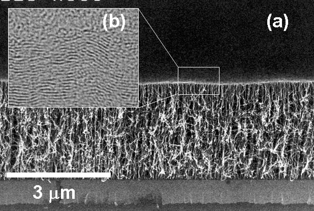
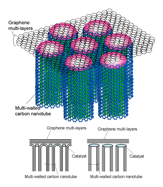
Figure 1. (a) Electron microscopic image (cross-sectional) of the new nano-scale carbon composite (b) Electron microscopic image of the graphene multi-layers Figure 2. Schematic view of the new nano-scale carbon composite (Lower image: Diagram of anticipated structure)

Background

Carbon nanotubes and graphene are both nano-scale structures consisting of carbon atoms. Graphene is a sheet-like hexagonal lattice of carbon atoms, while nanotubes can be described as graphene wrapped into a cylinder with a nano-scale diameter.

Despite the fact that both are made from the same carbon atoms, each has very distinct characteristics. Of any material found in nature, carbon nanotubes feature the highest thermal conductivity and mechanical strength as well as the ability to withstand the highest current density, making them an attractive material for wiring, heat dissipation, field electron emitters(4), and other potential applications. Research and development is underway to find technologies to synthesize carbon nanotubes at temperatures as low as approximately 400°C, a temperature that would enable its use in electronic devices vulnerable to heat. Since the discovery of its high electron mobility in 2004, graphene has become attractive as a channel material for future transistors. However, conventional methods for synthesizing graphene only work at temperatures over 700°C - considered too high for use in electronic devices - or involve a time-consuming and unreliable process of stripping away graphite crystals.

Fujitsu Laboratories is researching ways to develop electronic devices that take advantage of the superior properties of carbon nanostructures.

Overview of the new technology

In order to better understand the growth mechanism of carbon nanotubes, Fujitsu Laboratories conducted experiments using chemical vapor deposition, a technique in which a feedstock gas is heat-cracked in a vacuum chamber to synthesize film or structures on a substrate. This resulted in the formation and discovery of aligned growth(5)multi-walled carbon nanotubes(6) featuring layers of graphene (from a few layers to a few dozen) on top formed in a self-organizing way, thereby forming a complex composite (see Figure 1).

Carbon-based materials come in a variety of different forms that depend on how their atoms link together, such as zero-dimensional fullerenes(7), one-dimensional nanotubes, two-dimensional (2-D) graphene, and three-dimensional (3-D) diamonds. Complex structures consisting of zero-dimensional and one-dimensional elements, known as "peapod(8)" structures, have already been created. The new complex composite developed by Fujitsu Laboratories is the world's first composite featuring one-dimensional and two-dimensional elements based on graphene layers and nanotubes, which are perpendicularly connected. The composite was synthesized at the relatively low temperature of 510°C.

Results

Due to the fact that carbon nanotubes are linear, one-dimensional structures, in the two-dimensional directions perpendicular to the tube axis they have nearly no thermal or electrical conductivity between tubes. Graphene, on the other hand, possesses electrical and thermal conductivity across two dimensions. The newly-discovered carbon nanostructure is expected to have electrical conduction and thermal dissipation in all directions. Conventionally aligned-growth carbon nanotubes have had relatively poor uniformity in length, thus being inconsistent when joined in the upper areas and resulting in increased thermal and electrical resistance. As the new carbon nanostructures from Fujitsu Labs feature carbon nanotubes that nearly all connect to the graphene with good uniformity at their endpoints (see Figure 2), and since the graphene surface is planar, it is anticipated that the new carbon nanostructures will enable excellent electrical and thermal conductivity. This technology brings the application of graphene for electronic devices one step closer to practical use.

Future Developments

Fujitsu Laboratories will continue to explore the mechanisms by which complex carbon nanostructures form and elucidate their physical characteristics, in order to develop electronic device application technologies that take advantage of those characteristics. In addition, in the field of material sciences Fujitsu Laboratories will pursue the development of technologies to enable the formation of high-quality carbon nanostructures at a lower temperature.

Glossary and notes
1 Self-organizing structure:
Refers to a desired structure that self-forms naturally, without the need for complex controls.
2 Graphene:
A hexagonal lattice of carbon atoms. Graphite consists of layers of graphene stacked on top of each other.
3 Current-density tolerance:
The limit of high-density current that can flow through a material without changing its physical structure.
4 Field electron emitter:
A device that extracts electrons from a fixed surface employing an electrical field. Displays referred to as field-emission displays (FED) operate on the principle of electrons bumping up against fluorescent bodies, and causing them to emit light.
5 Aligned growth:
A growth pattern that grows perpendicular to a substrate.
6 Multi-walled carbon nanotube:
A type of carbon nanotube in which multiple graphene layers are arranged concentrically as a cylinder. Sizes vary in diameter from a few nanometers, to a few tens of nanometers.
7 Fullerene:
A molecule consisting of 60 carbon atoms arranged in a soccer-ball like structure.
8 Peapod:
A complex nanostructure consisting of fullerene laid out in a row inside a carbon nanotube. Named for its resemblance to a peapod.

About Fujitsu Laboratories

Founded in 1968 as a wholly owned subsidiary of Fujitsu Limited, Fujitsu Laboratories Ltd. is one of the premier research centers in the world. With a global network of laboratories in Japan, China, the United States and Europe, the organization conducts a wide range of basic and applied research in the areas of Multimedia, Personal Systems, Networks, Peripherals, Advanced Materials and Electronic Devices.
For more information, please see:http://jp.fujitsu.com/group/labs/en/


Press contacts:

Fujitsu Limited
Public and Investor Relations

Inquiries

Technical contacts:
Fujitsu Laboratories Ltd.
Nanotechnology R&D Center
Tel: +81-46-250-8234
E-mail:nano-mate@labs.fujitsu.com

http://www.fujitsu.com/global/news/pr/archives/month/2008/20080303-01.html

Ref:
http://www.japancorp.net/Article.Asp?Art_ID=17179