Showing posts with label CNT. Show all posts

Friday, December 3, 2010

OLED + CNT = KEESMANN

Here's the future - lighting AND TV - and remember - CNTs emitting electrons = KEESMANN:

ORGANIC LIGHT EMITTING DIODES WITH STRUCTURED ELECTRODES

Applicants: THE REGENTS OF THE UNIVERSITY OF CALIFORNIA

Abstract:
A cathode that contain nanostructures that extend into the organic layer of an OLED has been described. The cathode can have an array of nanotubes or a layer of nanoclusters extending out from its surface. In another arrangement, the cathode is patterned and etched to form protruding nanostructures using a standard lithographic process. Various methods for fabricating these structures are provided, all of which are compatible with large-scale manufacturing. OLEDs made with these novel electrodes have greatly enhanced electron injection, have good environmental stability.


[0008]As shown in the schematic in FIG. 1, an OLED 100 has an emissive layer 110, a transport layer 120, an anode 130 and a cathode 140, all on a substrate 150. The layers 110, 120 are made of organic semiconducting small molecules or polymers. When a voltage is applied across the OLED 100 such that the anode 120 is positive with respect to the cathode 140, the cathode 140 injects electrons 145 into the emissive layer 110 and the anode 130 injects holes 135 into the transport layer 120. The electrons 145 and the holes 135 move toward each other and they recombine. The recombination produces an emission of radiation 160 whose frequency is typically in the visible, may also be in the infrared and ultraviolet regions.


Nanotube and Nanocluster Cathodes

[0022]FIG. 2 is a schematic cross section drawing that shows an embodiment of the invention that uses a nanotube-based cathode. An OLED 200 has a cathode 240, a light-emitting organic layer 210, a transport layer 220, an anode 230, and a substrate 250. The anode 230 may be made of a transparent material, such as indium tin oxide (ITO) and the substrate 250 may be any known substrate such as plastic, glass, and the like. Light may be emitted in the direction of arrows 260 or in the opposite direction.

[0023]The cathode 240 has a plurality of nanostructures 242 extending outwardly into the light-emitting organic layer 210. The nanostructures 242 may be any type of structure such as nanotubes, nonorods, or nanoclusters. The nanostructures 242 can be nanotubes grown out from a cathode substrate 240. Alternatively, the nanostructures 242 can be nanoclusters deposited onto the cathode substrate 240.

[0024]Nanotubes are good field emitters because of their small tip radii, which can range from approximately one nanometer to as much as a micron. The smaller the tip radius the stronger the concentration of the electric field at the tip. A high electric field at the tip causes a high electron ejection rate, which results in very efficient ejection of electrons. In addition to improving electron injection from the cathode 240 to the light-emitting organic layer 210, the small tips and even distribution of the nanotubes 242 provide a balanced charge distribution in the device, reduce exciton quenching near the cathode 240, and allow for the use of lower voltages to achieve electron emission. Furthermore, carbon nanotubes are chemically stable, decreasing the environmental sensitivity of the cathode 240.

USPTO
WIPO

Thursday, June 4, 2009

A billion year ultra-dense nanotechnology memory chip

Posted: June 4, 2009

(Nanowerk News) When it comes to data storage, density and durability have always moved in opposite directions - the greater the density the shorter the durability. For example, information carved in stone is not dense but can last thousands of years, whereas today’s silicon memory chips can hold their information for only a few decades. Researchers with the U.S. Department of Energy’s Lawrence Berkeley National Laboratory (Berkeley Lab) and the University of California (UC) Berkeley have smashed this tradition with a new memory storage medium that can pack thousands of times more data into one square inch of space than conventional chips and preserve this data for more than a billion years!
This video shows an iron nanoparticle shuttle moving through a carbon nanotube in the presence of a low voltage electrical current. The shuttle’s position inside the tube can function as a high-density nonvolatile memory element. (Courtesy of Zettl Research Group)
“We’ve developed a new mechanism for digital memory storage that consists of a crystalline iron nanoparticle shuttle enclosed within the hollow of a multiwalled carbon nanotube,” said physicist Alex Zettl who led this research.
“Through this combination of nanomaterials and interactions, we’ve created a memory device that features both ultra-high density and ultra-long lifetimes, and that can be written to and read from using the conventional voltages already available in digital electronics.”
Zettl, one of the world’s foremost researchers into nanoscale systems and devices, holds joint appointments with Berkeley Lab’s Materials Sciences Division (MSD) and the Physics Department at UC Berkeley, where he is the director of the Center of Integrated Nanomechanical Systems. He is the principal author of a paper that has been published on-line by Nano Letters entitled: “Nanoscale Reversible Mass Transport for Archival Memory.” Co-authoring the paper with Zettl were Gavi Begtrup, Will Gannett and Tom Yuzvinsky, all members of his research group, plus Vincent Crespi, a theorist at Penn State University.
The ever-growing demand for digital storage of videos, images, music and text calls for storage media that pack increasingly more data onto chips that keep shrinking in size. However, this demand runs in sharp contrast to the history of data storage. Compare the stone carvings in the Egyptian temple of Karnak, which store approximately two bits of data per square inch but can still be read after nearly 4,000 years, to a modern DVD which can store 100 giga (billion) bits of data per square inch but will probably remain readable for no more than 30 years.
“Interestingly,” said Zettl, “the Domesday Book, the great survey of England commissioned by William the Conqueror in 1086 and written on vellum, has survived over 900 years, while the 1986 BBC Domesday Project, a multimedia survey marking the 900th anniversary of the original Book, required migration from the original high-density laserdiscs within two decades because of media failure.”
Zettl and his collaborators were able to buck data storage history by creating a programmable memory system that is based on a moveable part - an iron nanoparticle, approximately 1/50,000th the width of a human hair, that in the presence of a low voltage electrical current can be shuttled back and forth inside a hollow carbon nanotube with remarkable precision. The shuttle’s position inside the tube can be read out directly via a simple measurement of electrical resistance, allowing the shuttle to function as a nonvolatile memory element with potentially hundreds of binary memory states.
“The shuttle memory has application for archival data storage with information density as high as one trillion bits per square inch and thermodynamic stability in excess of one billion years,” Zettl said. “Furthermore, as the system is naturally hermetically sealed, it provides its own protection against environmental contamination.”
The nanoscale electromechanical memory device can write/read data based on the position of an iron nanoparticle in a carbon nanotube
The nanoscale electromechanical memory device can write/read data based on the position of an iron nanoparticle in a carbon nanotube. In this schematic, the memory devices are displaying a binary sequence 1 0 1 1 0 (Image: Zettl Research Group, Lawrence Berkeley National Laboratory and University of California at Berkeley.)
The low voltage electrical write/read capabilities of the memory element in this electromechanical device facilitates large-scale integration and should make for easy incorporation into today’s silicon processing systems. Zettl believes the technology could be on the market within the next two years and its impact should be significant.
“Although truly archival storage is a global property of an entire memory system, the first requirement is that the underlying mechanism of information storage for individual bits must exhibit a persistence time much longer than the envisioned lifetime of the resulting device,” he said. “A single bit lifetime in excess of a billion years demonstrates that our system has the potential to store information reliably for any practical desired archival time scale.”
The multiwalled carbon nanotube and enclosed iron nanoparticle shuttle were synthesized in a single step via pyrolysis of ferrocene in argon gas at a temperature of 1,000 degrees Celsius. The nanotube memory elements were then ultrasonically dispersed in isopropanol and deposited on a substrate. A transmission electron microscope provided high-resolution imaging in real time while the memory device was in operation. In laboratory tests, this device met all the essential requirements for digital memory storage including the ability to overwrite old data.
“We believe our nanoscale electromechanical memory system presents a new solution to the challenge of ultra-high density archival data storage,” Zettl said.
Source: Berkeley Lab

Source

Monday, May 25, 2009

Dense, long-lived iron-in-tube memory developed


EE Times Europe


Abstract

Abstract Image
We report on a simple electromechanical memory device in which an iron nanoparticle shuttle is controllably positioned within a hollow nanotube channel. The shuttle can be moved reversibly via an electrical write signal and can be positioned with nanoscale precision. The position of the shuttle can be read out directly via a blind resistance read measurement, allowing application as a nonvolatile memory element with potentially hundreds of memory states per device. The shuttle memory has application for archival storage, with information density as high as 1012 bits/in2, and thermodynamic stability in excess of one billion years.


LONDON — Researchers have developed a memory technology that should be ultra-dense compared with conventional silicon-based memories and that can store data for more than one billion years.

The information density can be as high as 1-terabit per square inch, according to a paper from the research team, led by Alex Zettl, of the University of California, Berkeley.

The memory is based on a nanoscale particle of iron that is contained and controllable positioned within a hollow carbon nanotube. The carbon nanotube is anchored to electrodes at either end and the nanoparticle can be moved, via an electrical write signal, and can be positioned anywhere within the tube.

The position of the nanoparticle can be read out via a resistance read measurement, allowing application as a nonvolatile memory element with potentially hundreds of memory states per device.

Source

Thursday, January 1, 2009

(WO/2009/002588) CARBON NANOTUBES FOR WIRELESS COMMUNICATION AND RADIO TRANSMISSION


Biblio. Data

Latest bibliographic data on file with the International Bureau
Pub. No.:
WO/2009/002588
International Application No.:
PCT/US2008/060130
Publication Date:31.12.2008 International Filing Date:11.04.2008
IPC: H03D 1/18 (2006.01)
Applicants:THE REGENTS OF THE UNIVERSITY OF CALIFORNIA [US/US]; 1111 Franklin Street, 5th Floor, Oakland, CA 94607-5200 (US) (All Except US).
BURKE, Peter, J. [US/US]; (US) (US Only).
RUTHERGLEN, Christopher, M. [US/US]; (US) (US Only).
Inventors:BURKE, Peter, J.; (US).
RUTHERGLEN, Christopher, M.; (US).
Agent:WORLEY, Eugene, R.; ORRICK HERRINGTON & SUTCLIFFE LLP, 4 Park Plaza, Suite 1600, Irvine, CA 92614-2558 (US).
Priority Data:
60/911,475
12.04.2007
US
Title: CARBON NANOTUBES FOR WIRELESS COMMUNICATION AND RADIO TRANSMISSION

Abstract:
Described herein are systems and methods in which a carbon nanotube (CNT) is used as a demodulator of amplitude-modulated (AM) signals. Due to the nonlinear current-voltage (I-V) characteristics of a CNT, the CNT induces rectification of an applied RF signal enabling the CNT to function as a demodulator of an amplitude-modulated (AM) RF signal. By properly biasing the CNT such that the operating point is centered on the maximum portion of the I-V curve, the demodulation effect of the CNT can be maximized. The present invention is useful for possible nanoscale wireless communications systems, e.g., nanoscale radios.


Source

Wednesday, November 12, 2008

University embarks on carbon nanotube data storage project, promises DRAM-like non-volatile memory

Trendwatch
By Rick C. Hodgin
Wednesday, November 12, 2008 03:30

Nottingham (UK) - Researchers at The University of Nottingham, one of UK's Top 10 universities, also ranking in the world's Top 100, stated yesterday that Project Nanodevice is underway. Their goal is to create molecular memory built of telescoping carbon nanotubes. "In this project a new device for storing information will be developed, made entirely of carbon nanotubes and combining the speed and price of dynamic memory with the non-volatility of flash memory."


Telescoping a carbon nanotube

The idea sounds simple enough; two carbon nanotubes of slightly different size, one resting inside the other like a two-member set of matryoshka (Russian dolls where each one has a smaller one inside). Electrical current will pass through the outer tube forcing the inner tube to telescope in or out. When out it will make contact with a remote electrode, thereby completing a circuit to create a binary one. When retracted the circuit will be broken - a binary zero.


Image
An artist's rendition of carbon nanotube memory in theory. (a) shows a full extended telescope and completed circuit representing a binary one. (b) shows a retracted telescope and an incomplete circuit creating a binary zero. Single-atom thick walls allow massive storage potential on the order of 10-100x more dense than modern flash memory with read/write speeds rivaling DRAM.


This kind of memory will be a physical displacement of matter, meaning something has to move in order to switch states. Tiny, rolled sheets of graphene make up the carbon nanotubes, and these exhibit molecular properties which make the movements extremely fast and reliable, at least theoretically.


Non-volatile, fast and friendly

Another advantage of this system is that the memory will be non-volatile. Just like flash memory today, it won't need any power to maintain its state. It should also be extremely resistant to G-force induced state changes, such as accidental droppage.

Even early generations of this technology should be as fast or faster than modern DRAM. Future computers using this kind of memory won't have a separate memory and hard disk for storage. Theirs will be a unified memory architecture built around this kind of storage medium, a new design paradigm for the instant on computer, one capable of continuous processing and data storage without ever swapping memory out to hard disk through paging. This one fact alone would greatly speed up our computer experience today.


"Project"ions

The project is being led by Dr. Elena Bichoutskaia, who said, "The electronics industry is searching for a replacement of silicon-based technologies for data storage and computer memory. Existing technologies, such as magnetic hard discs, cannot be used reliably at the sub-micrometre scale and will soon reach their fundamental physical limitations."

Her goals, and the goals of the research teams working on this project, is a new memory device. According to Bichoutskaia, a new carbon nanotube memory product will be produced, one that will replacing DRAM and flash. With research of this nature there are no timeframes.

Personally, I suggest a name for this creation, one in keeping with the finest traditions of existing memory naming conventions: CRAM (Carbon-nanotube RAM). "How many smaller nanotubes can I cram inside the bigger ones?" Perhaps future generations could move away from binary computers into ternary (or beyond) by having multiple tubes, like a real telescope.

Source

Friday, October 31, 2008

Hot nanotube sheets produce music on demand

16:08 31 October 2008
  • NewScientist.com news service
  • Colin Barras
Carbon nanotube speaker

Sheets made of carbon nanotubes behave like a loudspeaker when zapped with a varying electric current, say Chinese researchers. The discovery could lead to new generation of cheap, flat speakers.

Since the early 1990s, nanotubes have been intensively studied by researchers across the globe. The tiny structures are widely touted as potential drug delivery devices but might also be useful in more exotic gadgets including artificial photosynthesis devices and space elevators. But no one has thought to test their acoustic properties until now.

Shoushan Fan and his research team at Tsinghua University in Beijing, China, working with colleagues at Beijing Normal University, created a thin sheet by roughly aligning many 10-nanometer-diameter carbon nanotubes. When they sent an audio frequency current through the sheet, they discovered it acted as a loudspeaker.

A standard loudspeaker consists of three basic elements – a speaker cone, a voice coil and a magnet. The cone and coil are attached and sit in a permanent magnetic field created by the magnet. When an audio frequency current passes through the voice coil, it creates a temporary magnetic field, and the coil and cone shift relative to the permanent magnetic field. Those shifts induce vibrations in the air molecules near the speaker cone, generating sound.

How it works

Fan's team wondered whether the nanotube speaker behaved in a similar way. They used a laser vibrometer to look for vibrations in their nanotube speaker as it produced sound, but the sheet remained resolutely static throughout. Instead, they think that the nanotube speaker functions as a thermoacoustic device.

When an alternating current passes through the nanotube sheet, the sheet alternates between room temperature and 80 °C. Those rapid temperature oscillations lead to pressure oscillations in the air next to the film. It is those thermally induced pressure oscillations that are responsible for the sound, rather than any physical movement of the nanotube sheet itself.

In fact, the researchers realised this phenomenon was first observed over a century ago independently by William Henry Preece and Karl Ferdinand Braun. Those nineteenth century researchers realised they could get sound from a thin metal foil by passing an alternating current through it, a discovery that led to the invention of a device called the "thermophone".

But the thermophone produced a very weak sound, whereas the nanotube sheets can be very loud (see video). That's because of the unusual properties of carbon nanotubes, says Fan. "A key parameter that determines the sound generation efficiency is the heat capacity per unit area," he says. Put simply, that's a measure of how much heat energy must be applied to a material to raise its temperature. The heat capacity per unit area of a carbon nanotube sheet is 260 times smaller than that of a platinum foil sheet. That means a nanotube sheet can generate sound waves 260 times more efficiently than a platinum sheet, and so produce a much louder sound.

'Singing jackets'

The nanotube loudspeakers have several key advantages over standard speaker systems, says Fan. "Conventional loudspeakers which [produce sound] due to the vibration of the cone will fail to emit sound if the cone is broken," he says. "The carbon nanotube loudspeaker does not vibrate, which means it will still emit sound if part of the film is broken."

The flexible nanotube sheets can be stretched or flexed into complicated shapes and they still produce sound, Fan says. When fully stretched, the sheets are transparent and so they could be attached to the front of an LCD screen to replace standard speakers.

Watch a video of a carbon nanotube speaker being stretched

But more exotic uses might see nanotube sheets stitched into clothing to create "singing and speaking jackets", Fan's team thinks.

Cees Dekker, a nanoscience expert at Delft University of Technology in the Netherlands, finds the new study very interesting. "It's just amazing how widespread the diversity of applications of these nanotubes are," he says.

Journal reference: Nano Letters (DOI: 10.1021/nl802750z)

Source

Thursday, May 29, 2008

Major Advance in Manufacture of El-Mul’s Nanotube-Based Field Emitter

WEBWIRE – Thursday, May 29, 2008
Contact Information
Bob Rosenbaum
Marketing Director
El-Mul Technologies Ltd
+972 8-943-4184
bob.rosenbaum@el-mul.com

Achievement details to be presented at 2008 Conference
of the Nanoscience and Technology Institute in Boston.

YAVNE, ISRAEL (29 May 2008) – El-Mul Technologies announced today that it has gained critical knowledge that will allow commercial manufacture of its proprietary carbon nanotube (CNT) based field emission device. This achievement enables development of the device for a variety of industrial applications, including production of E-beam sources to be used primarily in analytical instruments and semiconductor tools.

Details of the achievement will be presented on June 3 at the 2008 Conference of the Nanoscience and Technology Institute (NSTI) to be held in Boston, by Mr. Sagi Daren, El-Mul’s Nano Electron Source (NES) project manager.

“Today we are offering a working industrial process to manufacture complex CNT-based electron sources with outstanding performance for real life applications,” Dr. Armin Schon, CEO of El-Mul Technologies, announced. “We can now custom design and produce sources for various applications and we will expand our offerings in the near future, both in our home markets and elsewhere.”

The company is focusing on design and manufacture of E-beam sources in two areas: well-characterized fine beam applications based on single CNT emitters, and high-current broad beam applications based on multi-beam CNT emitter arrays. Marketed as the E-Beam On-a-Chip™ platform, El-Mul’s first product is currently undergoing testing with a European partner.

Schon noted that early stages of El-Mul’s CNT electron source project were greeted with skepticism. “I heard many critical comments about the technological difficulties of such an endeavor. Today we can show that we have overcome the biggest challenge of all – high yield manufacturing.” Schon also praised the project team members. “We’ve been successful because we’ve harnessed the best properties of Israel’s high tech culture: highly qualified and motivated team members with very high tolerance for risk and disappointment, working alongside management that has the long-term vision to guide a very challenging process through to its resolution.”

El-Mul’s initial electron source device is targeted primarily for next generation scanning electron microscope (SEM) and transmission electron microscope (TEM) systems. The new device is expected to result in 30 percent higher resolution, a four-fold increase in scanning speeds, and a significant cost reduction in both manufacturing and maintenance of SEM and TEM systems.

El-Mul’s patented approach creates a MEMS-based electron source that results in superior beam brightness, narrower energy spread and smaller source size than conventional electron emitter devices. To manufacture the new device, El Mul has also developed a proprietary chemical vapor deposition (CVD) process that grows single CNT emitters inside cathode wells 4 microns deep.

Among potential application markets for the E-Beam On-a-Chip™ platform are: sub 40 nm E beam lithography, metrology and inspection tools (for semiconductor manufacturing); X ray and mass spectrometry tools (for medical and life sciences); and field emission displays.

CNT-based electron source device R&D has been funded through strategic partnerships and by the Office of the Chief Scientist in Israel’s Ministry of Industry and Trade. El Mul holds US and international patents for its R&D in this area.

El-Mul Technologies has over 16 years experience in the design and manufacture of electron and ion detectors for a wide variety of industries and research environments, and is recognized today as a leading solutions provider for nanotechnology toolmakers. El-Mul has pioneered nanoscale devices since 1999.


Source


29 May 2008

E-Beam On-a-Chip™ Device Achievements Announced

El-Mul to present major advances in the manufacture of it's patented carbon nanotube-based electron beam source platform at the NSTI 2008 conference in Boston.


Download Press Release (PDF, 152 KB)

Request more information


Source

El-Mul US patent reference:

United States Patent 6,512,235
Eitan , et al. January 28, 2003

Nanotube-based electron emission device and systems using the same

Abstract

A device that produces an electron beam with high optical quality for processing a sample, is presented. The optical quality is manifested by very high brightness and low energy spread. The device includes an electron source device comprising an electrode in the form of a shaped first layer, preferably in the form of a conducting crater carrying at least one nanotube, and an extracting electrode, which is formed with at least one aperture and is insulated from the firs layer. The source can be used in any column that requires such properties. The column according to the invention may be a full size or a miniature electron microscope, a lithography tool, a tool used for direct writing of wafers or a field emission display.


Inventors: Eitan; Guy (Menorah, IL), Zik; Ory (Tel Aviv, IL), Rosenblatt; David (Philadelphia, PA)
Assignee: El-Mul Technologies Ltd. (Yavne, IL)
Appl. No.: 09/561,958
Filed: May 1, 2000

Extract:
Since the electron source device that is based on fiber(s), e.g., nanotube(s), in a conducting crater emits with sufficient brightness to be used in electron microscopy, it is evident that a matrix of craters is suitable for a field emission display, where each beamlet correspond to a pixel. Thus, the current invention is also suitable for flat panel displays.

The advantages of the present invention are thus self-evident The electron source device according to the invention enables to solve various constructional and operational problems of electron source device based systems, such as electron microscopes, lithography tools and flat displays. Due to the small size of the nanotube-based electron source device and relaxed vacuum requirements, the entire system can have a desirably small footprint, and can allow for assembling a multiple-column arrangement to be advantageously used in various applications. Due to the elevated optical performance of the electron gun and reduced chromatic and spherical aberrations of the associated electron beam, the performance of the system is significantly improved. In fact, the invention allows to the useful utilization of nanotubes in an electron gun. The use of "patterned" cathode-electrode, and preferably by means of the same anode-electrode, the construction and operation of a lithography tool utilizing such an electron source device is significantly improved.

Source

WO/2001/084130 (PCT equivalent)

Tuesday, May 27, 2008

Method of fabricating memory device utilizing carbon nanotubes

United States Patent 7,378,328 Choi, et al., May 27, 2008

Abstract

A fast, reliable, highly integrated memory device formed of a carbon nanotube memory device and a method for forming the same, in which the carbon nanotube memory device includes a substrate, a source electrode, a drain electrode, a carbon nanotube having high electrical and thermal conductivity, a memory cell having excellent charge storage capability, and a gate electrode. The source electrode and drain electrode are arranged with a predetermined interval between them on the substrate and are subjected to a voltage. The carbon nanotube connects the source electrode to the drain electrode and serves as a channel for charge movement. The memory cell is located over the carbon nanotube and stores charges from the carbon nanotube. The gate electrode is formed in contact with the upper surface of the memory cell and controls the amount of charge flowing from the carbon nanotube into the memory cell.

Inventors: Choi; Won-bong (Yongin, KR), Yoo; In-kyeong (Suwon, KR), Chu; Jae-uk (Gwangmyeong, KR)

Assignee: Samsung Electronics Co., Ltd. (Suwon, Kyungki-do, KR)

http://tinyurl.com/56r5a3

I'm all for it - the more the merrier - Keesmann agrees, I hope.

Phase changeable memory devices including carbon nano tubes

United States Patent 7,378,701 Hideki May 27, 2008, Samsung

Abstract

An integrated circuit phase changeable memory device includes an integrated circuit substrate, a first electrode on the integrated circuit substrate, and a second electrode on the integrated circuit substrate and spaced apart from the first electrode. A carbon nano tube and a phase changeable layer are serially disposed between the first and second electrodes. An insulating layer can include a contact hole and the carbon nano tube may be provided in the contact hole. Moreover, the phase changeable layer also may be provided at least partially in the contact hole. A layer also may be provided at least partially surrounding the carbon nano tube in the contact hole. Related fabrication methods also are provided.

Inventors: Hideki; Horii (Seoul, KR)

Assignee: Samsung Electronics Co., Ltd. (KR)

http://tinyurl.com/4t5yd4

Not sure if this is coincidental, but here it is - same issue day as UMK's offering and very similar. I think the USPTO lets them slug it out together outside the patent office as to who owns what. UMK's was magnetic while this one is phase change so that could be the distinction.

Large-capacity magnetic memory using carbon nano-tube

United States Patent 7,379,326 Ushida,et al., May 27, 2008

[[Note - Is this CNT emitting? If it is Keesmann applies! It could be big!!!]]

Abstract

A high-capacity magnetic memory capable of writing and reading a magnetic record in/from a magnetic recording film according to a perpendicular magnetic recording system at a high speed in a purely-electrically random access manner. In the magnetic memory, a writing-magnetic-field generating means 62 and a writing word line 43 are disposed relative to a perpendicular magnetic recording film 50, and a reading/writing bit-line conductor 41, a magnetoresistive-effect element 20 and a reading word lead conductor 42 are laminated in order on a probe substrate opposed to the perpendicular magnetic recording film 50. A magnetic probe 30 composed of a carbon nanotube containing a soft magnetic material is disposed relative to the magnetoresistive-effect element 20 in a standing manner, and electrically connected to the reading/writing bit-line conductor. During a writing operation, a micro-discharge is generated in a micro-gap G between the edge of the magnetic probe and the magnetic recording film under a writing magnetic field to allow a writing current to flow through the micro-gap G so as to heat a micro-region of the magnetic recording film in such a manner that it goes through its Curie point to thereby become magnetized in the direction of the recording magnetic field to form a magnetic record therein. During a reading operation, the magnetic record is read out through the magnetic probe in accordance with a current variation in the magnetoresistive-effect element.

Inventors: Ushida; Takashi (Furukawa, JP), Mori; Nobuyuki (Furukawa, JP), Kamijo; Yoshimi (Furukawa, JP), Okazaki; Akihiro (Furukawa, JP), Mitsuzuka; Akira (Furukawa, JP), Hatakeyama; Rikizou (Furukawa, JP), Ido; Hideaki (Furukawa, JP), Nakajima; Ko (Furukawa, JP), Takoshima; Takehiro (Furukawa, JP)

Assignee: UMK Technologies Co., Ltd. (Furukawa-shi, JP)

The nano-magnetic probe 30 is disposed in opposed relation to the perpendicular magnetization film 50 through a micro-gap G, and the space S therebetween is sealed in a vacuum or depressurized state. If the conditions for generating a micro-discharge are satisfied, the space may be maintained under an inert atmosphere instead of the depressurized state. [[Sounds like electron emission is present!]]

http://tinyurl.com/4t5yd4

If this is as big as I think it is or could/will be, it could be worth a pretty penny to us and Keesmann. Don't ya think? Then again it might just be another disappointment - we can handle those!!!!!! We are used to it. ;-)

Refs:
http://www.wipo.int/pctdb/en/wo.jsp?wo=2004001851
http://www.freepatentsonline.com/EP1533846.html

Sunday, May 11, 2008

Polynano carbon nanotube field emission device

Polynano Glass---( Nano Moving Display Glass )

Polynano carbon nanotube field emission device (CNT-FED) features perfect flat outer screen surface, flat rear screen, very thin thickness, high beam current output of carbon Nanotube emission cathode, circle phosphor dot screen anode, monochrome output, see-through type , wide-environmental operation application. Monochrome display and image interface application.

Snipped from here:
http://www.glassonweb.com/articles/artic...

Finally something to generate some royalty revenue for Keesmann and ANHI (Applied Nanotech Holdings Inc.)=(Nano-Proprietary - NNPP)!

Long time coming but welcomed with open arms and pocketbooks.

Ya think? ;-) Surely Bijou is all over this like a hawk in heat.

OTOH.............???????

Just in case NOT here are the company particulars:
Polytron Technologies, Inc.
http://www.polytron.com.tw/company.php?l...

Polytron Technologies Inc. is a subsidiary of Polytronix, Inc.:
http://www.polytronix.com/
http://www.polytron.com.tw/
http://www.polytron.com.tw/product_small...
Polytron Technologies, Inc.
330 No.67, Taode Road., Taoyuan City, 330, Taiwan
Tel:+886-3-3712958 FAX:+886-3-3712968
sam@polytron.com.tw

POLYTRONIX INC.

Contact Information

805 Alpha Drive
Richardson, Texas 75081-2861

Toll Free: 1-800-904-7045
Phone: 972-238-7045
Fax: 972-644-0805

For technical and engineering questions,
contact: engineering@polytronix.com

For product information and availability,
contact: sales@polytronix.com

POLYTRONIX INC. URL:

http://www.polytronix.com/contacts.htm

TEXAS, eh!!!!

Howdy, pardner.

Tuesday, May 6, 2008

The high contrast ratio and fast response time of a liquid crystal display lit by a carbon nanotube field emission backlight unit

Young Chul Choi et al 2008 Nanotechnology 19 235306 (5pp) doi: 10.1088/0957-4484/19/23/235306 Help

PDF (943 KB) | References


Young Chul Choi, Ji Won Lee, Su Kyung Lee, Mun Seok Kang, Chang Soo Lee, Kyu Won Jung, Ji Hong Lim, Jong Woon Moon, Myung Ick Hwang, Il Hwan Kim, Yun Hee Kim, Byong Gon Lee, Hyung Rae Seon, Sang Jin Lee, Jong Hwan Park, Yong C Kim and Hun Soo Kim
Display Laboratory 3 Group, Corporate R&D Center, Samsung SDI, 428-5, Gongse-dong, Giheung-gu, Yongin, Gyeonggi 446-577, Republic of Korea
E-mail: hs88.kim@samsung.com

Abstract. We report on the fabrication of a carbon nanotube field emission backlight unit (CNT-BLU) and its application for liquid crystal displays (LCD). The CNT-BLU was operated with locally controllable luminance and impulse-type scanning. The local luminance control, which is based on a very small block size of 1 cm2, consisted of local dimming and local brightening. This resulted in the contrast ratio of the LCD-TV to be as high as 300 000:1. A fast response time of ~5.7 ms was also achieved from the LCD-TV lit by CNT-BLU, originating from the impulse-type scanning. In addition, the CNT-BLU showed long-term emission stability and high luminance uniformity.

Print publication: Issue 23 (11 June 2008)
Received 7 March 2008, in final form 10 April 2008
Published 6 May 2008

Source

Conclusion - from PDF:

4. Conclusion
We have developed an FE-BLU using a CNT emitter (CNTBLU), and then analyzed its field emission characteristics including emission current, stability and uniformity. Well distributed CNTs were precisely integrated into gate holes through simple photolithography and a surface treatment process. The CNT-BLU generated high emission current with long-term stability and the observed emission uniformity was high enough to be used for an LCD-TV. The image characteristics of an LCD-TV lit by the CNT-BLU were evaluated and compared with those by a CCFL. Compared with a CCFL backlight, at least 200 times enhanced contrast ratios and three times improved response times were demonstrated by using the CNT-BLU. These were achieved by fine local luminance control and impulse-type scanning, respectively. Achieving these technologies using CNT emitters is believed to be very promising for the next-generation LCDs with excellent image characteristics.

Monday, April 14, 2008

How falling spaghettis could lead to more complex nanotechnology self-assembly

Posted: April 14, 2008

(Nanowerk Spotlight) Self-assembly and self-organization are terms (read this discussion about the difference between the two) used to describe processes in which a disordered system of pre-existing components forms an organized structure or pattern as a consequence of specific, local interactions among the components themselves, without external direction. Self-organizing processes are common throughout nature and involve components from the molecular (e.g. protein folding) to the planetary scale (e.g. weather systems) and even beyond (e.g. galaxies). Self-assembly has become an especially important concept in nanotechnology. As miniaturization reaches the nanoscale, conventional manufacturing technologies fail because it has not been possible (yet) to build machinery that assembles nanoscale components into functional devices (for more on this, read Mind the gap - nanotechnology robotics vision versus lab reality). Until robotic assemblers capable of nanofabrication can be built, self-assembly - together with chemical synthesis - will be the necessary technology to develop for bottom-up fabrication.
The stability of covalent bonds enables the synthesis of almost arbitrary configurations of up to 1000 atoms. Larger molecules, molecular aggregates, and forms of organized matter more extensive than molecules cannot be synthesized bond-by-bond. Self-assembly is one strategy for organizing matter on these larger scales (Source).
The key to using self-assembly as a controlled and directed fabrication process lies in designing the components that are required to self-assemble into desired patterns and functions. Self-assembly reflects information coded – as shape, surface properties, charge, polarizability, magnetic dipole, mass, etc. – in individual components; these characteristics determine the interactions among them.
"It has long been recognized that whereas self-organization near thermodynamic equilibrium tends to attenuate fluctuations, leading to relatively simple geometries, self-organization far from equilibrium can amplify fluctuations into coherent oscillations, leading to much more complex structures" Dr. Ernesto Joselevich tells Nanowerk. While much of the work on molecular self-assembly has focused on equilibrium systems, leading to highly ordered arrays such as crystals, Joselevich points out that this universal principle of 'order through fluctuations' has not yet been widely applied to the self-assembly of complex structures at the nanoscale – although it is the essence of the emergence of order, complexity and life in the universe in spite of the second law of thermodynamics.
Joselevich, a Senior Scientist in the Department of Materials and Interfaces at the Weizmann Institute of Science in Israel, together with PhD students Noam Geblinger and Ariel Ismach, has just published a report in Nature Nanotechnology on an intriguing new type of nanotube structures – serpentines – strikingly more complex than those observed before (Self-organized nanotube serpentines).
"Here we show that combined surface- and flow-directed growth enable the controlled formation of uniquely complex and coherent geometries of single-walled carbon nanotubes, including highly oriented and periodic serpentines and coils" Joselevich explains to Nanowerk. "We propose a mechanism of non-equilibrium self-organization, in which competing dissipative forces of adhesion and aerodynamic drag induce oscillations in the nanotubes as they adsorb on the surface."
carbon nanotube serpentines
SEM image of a nanotube serpentine (Reprinted with permission from Nature Publishing Group)
So far, controlled formation of complex nanotube geometries like rings and loops has been achieved by directed assembly of preformed nanotubes, using templates and microfluidics. In these cases, the alignment was solely determined by the surface of the template, and not affected by external forces such as electric fields or gas flow.
"A few years ago, in experimenting with the growth of carbon nanotubes along atomic steps, we produced arrays of perfectly straight and parallel nanotubes" Joselevich explains the background to his latest paper. "While playing with different substrates, we noticed a few serpentines on some of our samples of single-walled carbon nanotubes (SWCNTs) grown on quartz. This phenomenon could not be explained by our previous mechanism of growth along steps, because it did not make sense why a nanotube growing along a step would suddenly make a U-turn, then after a certain length make another U-turn in the opposite direction, and after precisely the same length make an opposite U-turn, and so on. The serpentine shape was a highly complex organized structure whose formation was a mystery for us.
"One evening, I saw my toddler son playing with spaghetti, and realized that when the spaghetti fell on a bamboo mat, it fell down making wiggles and produced serpentine shapes very similar to those of the nanotubes serpentines that we had observed in our lab experiments."

'Falling-spaghetti mechanism' for the formation of self-organized nanotube serpentines
Joselevich's team hypothesized that the serpentines could form in a two-step mechanism, where the nanotubes first grow standing up from the surface, and at a later stage adsorb on the surface in an oscillatory fashion along the steps. "Once we understood this" he says, "we patterned the catalyst on stripes of amorphous silicon oxide to prevent growth along the steps of the quartz. Then we were able to fabricate thousands of nanotube serpentines and could systematically study their formation and properties."
The serpentines are made of SWCNTs with a very low concentration of defects and appear to have exactly the same electronic properties as regular SWCNTs. Hence they are expected to be either metallic or semiconducting depending on their diameter and chirality. The team's data show that the diameter and chirality remain constant along the entire serpentine, which can be longer than one millimeter.
Joselevich notes that the serpentine shape has very interesting geometric properties. It provides maximum coverage of a certain area by a single line and it packs the maximum contour length of a line on a minimum area. "Hence, you find this shape in many daily useful objects like heating and cooling devices, illumination and irrigation systems, etc. We would like to produce nanodevices that take advantage of the serpentine shape for analogous applications in a miniature size."
The Weizmann Institute team's self-organizing nanotube serpentines is a dramatic example of non-equilibrium self-organization or 'order through fluctuations' at the nanoscale. Joselevich believes that if we learn how to produce complex structures through non-equilibrium self-organization we will be able to produce a lot of new functional nanosystems with potential applications not previously thought possible.
By Michael Berger. Copyright 2008 Nanowerk LLC

Link

Thursday, March 20, 2008

Sony/Patents/Nanowire/FED/CNT/Display

1)
United States Patent Application
20080067915

Ishida; Takehisa ; et al.

March 20, 2008
Electron emitter and a display apparatus utilizing the same

Abstract

A field effect electron emitting apparatus using nano-wire electron emitters is disclosed where each nano-wire electron emitter may be grown in a pore of an insulating layer and/or may have at least a portion exposed from the pore. A method of manufacturing a field effect electron emitting apparatus is also disclosed. The field effect electron emitting apparatus may be used in a display.

Claims
1. A field effect electron emitting apparatus comprising a cathode, an insulating layer on or adjacent to the cathode having an array of pores, and a grown nano-wire electron emitter in each pore, each nano wire electron emitter connected to the cathode.

26. A field effect display comprising a field effect electron emitting apparatus as claimed in claim 1, and a phosphor coated screen on or spaced parallel to the field effect electron emitting apparatus.

Inventors:
Ishida; Takehisa; (Singapore, SG) ; Ng; Wei B.; (Singapore, SG)

Assignee Name and Adress:
Sony Corporation
Tokyo
JP

http://tinyurl.com/yq4jgd

2)
United States Patent Application 20080067912

Ishida; Takehisa
March 20, 2008
Electron emitter and a display apparatus utilizing the same

Abstract

A field effect electron emitting apparatus is disclosed comprising an insulating layer having an array of pores, each pore has at least one nano-wire electron emitter which is shorter than the pore and/or each pore may have a plurality of nano-wire electron emitters. A method of manufacturing a electron emitting array is also disclosed. The field effect electron emitting apparatus may be used in a display.
Inventors: Ishida; Takehisa; (Singapore, SG)

Assignee Name and Adress:
Sony Corporation
Tokyo
JP

Claims
1. A field effect electron emitting apparatus comprising a cathode, an insulating layer on or adjacent to the cathode having an array of pores, at least one nano-wire electron emitter within each pore, each nano-wire electron emitter being shorter than the pore and connected to the cathode, and a gate electrode on or adjacent to the insulating layer.

2. A field effect electron emitting apparatus comprising a cathode, an insulating layer on or adjacent to the cathode having an array of pores, a plurality of nano-wire electron emitters in each pore connected to the cathode, a gate electrode on or adjacent to the insulating layer.

3. A field effect electron emitting apparatus comprising a cathode, an insulating layer on or adjacent to the cathode having an array of pores, at least one electron emitter within each pore, each electron emitter being shorter than the pore and connected to the cathode, a gate electrode on or adjacent to the insulating layer, and a secondary electron emission (SEE) layer on the sidewall of each pore.

4. The electron emitting apparatus as claimed in claim 1 wherein each nano-wire is a carbon nano-tube (CNT).

http://tinyurl.com/35e5os

Sony, god love 'em, they make Canon look like amateurs and will bury SED!!

CNTs are THE future of displays - Sony has spoken...and when Sony speaks, I listen. What was that last bit, Sony??...."Buy NNPP!!!"......???

Saturday, March 15, 2008

SED Figure with 'nanotube' indication

Does SED include carbon nanotubes? This drawing-description seems to indicate so.
This was discussed today here LINK. I include this on my blog for the record and
easy retrieval in the future.


Wednesday, March 12, 2008

Nanotubes Show Their Strengths in Polymer Fibres

Researchers at Queen Mary, University of London and Nanoforce Technology Ltd. in the UK, have successfully produced single-walled nanotube reinforced polymer fibres and tapes that are as strong as theory predicts.

The work shows for the first time the true reinforcing potential of single-walled carbon nanotubes (SWNTs) with effective properties of nanotubes in composites, which are close to their theoretical values.

Prof. Ton Peijs, who heads the research team said: "The problem with carbon nanotubes has always been that despite their amazing potential of becoming the ultimate reinforcing fibre for the next generation of high-performance composites, their success in actually delivering these mechanical properties when embedded in polymer composites has been limited. Despite promises of tensile strengths of 100 GPa or more – 15 to 40 times higher than carbon fibres – their efficiency after embedding them in polymer matrices has often been poor with effective reinforcing properties not far better than those of carbon fibres”.

Dr. Zhujuang Wang, who processed and characterized the new nanocomposite fibres and tapes during her PhD study at QMUL, says that in order to get the most out of nanotubes the composite need to exhibit a good dispersion as well as good interfacial interaction of the nanotubes with the hosting matrix. Moreover, similar to polymer molecules the excellent intrinsic mechanical properties of nanotubes can only be expected if they are all fully aligned. The QMUL team has explored many different nanotube/polymer combinations but the best results were obtained for a system based on poly(vinyl alcohol) (PVA) and SWNTs. Using solid-state drawing technology the team showed that they can effectively align nanotubes along the polymer fibre axis and triple the tensile strength of the PVA fibre or tape with the addition of only 1 wt.% of SWNTs. Further analysis of the materials showed that the stress carried by the SWNTs in these oriented PVA composites was very close to the theoretical tensile strength of nanotubes, indicating the exceptionally high reinforcing efficiency of the SWNTs in these materials.

In order to make the research a commercial success still some significant further developments are needed. Peijs said: “Although our work shows that indeed the impressive mechanical properties of nanotubes can effectively be translated into high-performance composites, the challenge is still to make a nanocomposite fibre of record breaking strength. We expect that in order to make such a fibre we will need to incorporate at least 5 wt.% of perfectly aligned and dispersed SWNTs in a highly oriented PVA fibre. So far we have only achieved good dispersions up to 1 wt.% of nanotubes, which makes that our current nanocomposite fibres and tapes have still significantly lower strengths than ultra-strong carbon fibres possessing strengths up to 7 GPa. If dispersion problems at high nanotube loadings can be overcome, nanocomposite fibres with strengths exceeding those of the strongest carbon fibre are possible. Such fibres can find their way in a large range of advanced composite materials, ranging from structural materials in sports equipment and aircraft to anti-ballistics.

The researchers published their work in Nanotechnology in a paper entitled “Extraordinary reinforcing efficiency of single-walled carbon nanotubes in oriented poly (vinyl alcohol) tapes”.

http://www.iop.org/EJ/abstract/0957-4484/18/45/455709/

Publication Date: 11/03/2008

http://www.netcomposites.com/news.asp?4866

Monday, March 3, 2008

Composite of carbon nanotubes and graphene

Atsugi, Japan, March 3, 2008 — Fujitsu Laboratories Ltd. today announced the successful formation of a new nano-scale carbon composite featuring a self-organizing structure(1), by combining carbon nanotubes and graphene(2) which are both nano-scale carbon structures. The newly-discovered composite structure is synthesized at a temperature of 510 °C, cooler than for conventional graphene formed at temperatures too high for electronic device applications, thereby paving the way for the feasible use of graphene as a material suitable for future practical use in electronic devices which are vulnerable to heat. Carbon nanotubes have properties including high thermal conductivity and high current-density tolerance(3), while graphene is known for its high electron mobility. Carbon nanostructures combining these two materials hold the promise of creating new potential for material research and applications.

Details of this technology will be presented at the 34th Fullerene Nanotubes General Symposium to be held from March 3 to March 5 in Nagoya, Japan.

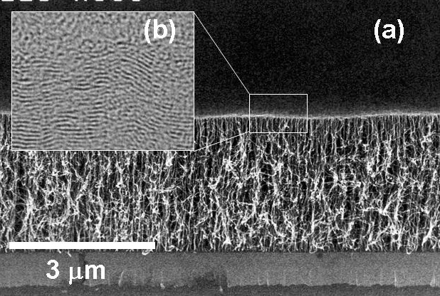
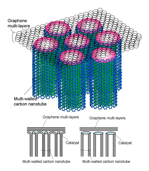
Figure 1. (a) Electron microscopic image (cross-sectional) of the new nano-scale carbon composite (b) Electron microscopic image of the graphene multi-layers Figure 2. Schematic view of the new nano-scale carbon composite (Lower image: Diagram of anticipated structure)

Background

Carbon nanotubes and graphene are both nano-scale structures consisting of carbon atoms. Graphene is a sheet-like hexagonal lattice of carbon atoms, while nanotubes can be described as graphene wrapped into a cylinder with a nano-scale diameter.

Despite the fact that both are made from the same carbon atoms, each has very distinct characteristics. Of any material found in nature, carbon nanotubes feature the highest thermal conductivity and mechanical strength as well as the ability to withstand the highest current density, making them an attractive material for wiring, heat dissipation, field electron emitters(4), and other potential applications. Research and development is underway to find technologies to synthesize carbon nanotubes at temperatures as low as approximately 400°C, a temperature that would enable its use in electronic devices vulnerable to heat. Since the discovery of its high electron mobility in 2004, graphene has become attractive as a channel material for future transistors. However, conventional methods for synthesizing graphene only work at temperatures over 700°C - considered too high for use in electronic devices - or involve a time-consuming and unreliable process of stripping away graphite crystals.

Fujitsu Laboratories is researching ways to develop electronic devices that take advantage of the superior properties of carbon nanostructures.

Overview of the new technology

In order to better understand the growth mechanism of carbon nanotubes, Fujitsu Laboratories conducted experiments using chemical vapor deposition, a technique in which a feedstock gas is heat-cracked in a vacuum chamber to synthesize film or structures on a substrate. This resulted in the formation and discovery of aligned growth(5)multi-walled carbon nanotubes(6) featuring layers of graphene (from a few layers to a few dozen) on top formed in a self-organizing way, thereby forming a complex composite (see Figure 1).

Carbon-based materials come in a variety of different forms that depend on how their atoms link together, such as zero-dimensional fullerenes(7), one-dimensional nanotubes, two-dimensional (2-D) graphene, and three-dimensional (3-D) diamonds. Complex structures consisting of zero-dimensional and one-dimensional elements, known as "peapod(8)" structures, have already been created. The new complex composite developed by Fujitsu Laboratories is the world's first composite featuring one-dimensional and two-dimensional elements based on graphene layers and nanotubes, which are perpendicularly connected. The composite was synthesized at the relatively low temperature of 510°C.

Results

Due to the fact that carbon nanotubes are linear, one-dimensional structures, in the two-dimensional directions perpendicular to the tube axis they have nearly no thermal or electrical conductivity between tubes. Graphene, on the other hand, possesses electrical and thermal conductivity across two dimensions. The newly-discovered carbon nanostructure is expected to have electrical conduction and thermal dissipation in all directions. Conventionally aligned-growth carbon nanotubes have had relatively poor uniformity in length, thus being inconsistent when joined in the upper areas and resulting in increased thermal and electrical resistance. As the new carbon nanostructures from Fujitsu Labs feature carbon nanotubes that nearly all connect to the graphene with good uniformity at their endpoints (see Figure 2), and since the graphene surface is planar, it is anticipated that the new carbon nanostructures will enable excellent electrical and thermal conductivity. This technology brings the application of graphene for electronic devices one step closer to practical use.

Future Developments

Fujitsu Laboratories will continue to explore the mechanisms by which complex carbon nanostructures form and elucidate their physical characteristics, in order to develop electronic device application technologies that take advantage of those characteristics. In addition, in the field of material sciences Fujitsu Laboratories will pursue the development of technologies to enable the formation of high-quality carbon nanostructures at a lower temperature.

Glossary and notes
1 Self-organizing structure:
Refers to a desired structure that self-forms naturally, without the need for complex controls.
2 Graphene:
A hexagonal lattice of carbon atoms. Graphite consists of layers of graphene stacked on top of each other.
3 Current-density tolerance:
The limit of high-density current that can flow through a material without changing its physical structure.
4 Field electron emitter:
A device that extracts electrons from a fixed surface employing an electrical field. Displays referred to as field-emission displays (FED) operate on the principle of electrons bumping up against fluorescent bodies, and causing them to emit light.
5 Aligned growth:
A growth pattern that grows perpendicular to a substrate.
6 Multi-walled carbon nanotube:
A type of carbon nanotube in which multiple graphene layers are arranged concentrically as a cylinder. Sizes vary in diameter from a few nanometers, to a few tens of nanometers.
7 Fullerene:
A molecule consisting of 60 carbon atoms arranged in a soccer-ball like structure.
8 Peapod:
A complex nanostructure consisting of fullerene laid out in a row inside a carbon nanotube. Named for its resemblance to a peapod.

About Fujitsu Laboratories

Founded in 1968 as a wholly owned subsidiary of Fujitsu Limited, Fujitsu Laboratories Ltd. is one of the premier research centers in the world. With a global network of laboratories in Japan, China, the United States and Europe, the organization conducts a wide range of basic and applied research in the areas of Multimedia, Personal Systems, Networks, Peripherals, Advanced Materials and Electronic Devices.
For more information, please see:http://jp.fujitsu.com/group/labs/en/


Press contacts:

Fujitsu Limited
Public and Investor Relations

Inquiries

Technical contacts:
Fujitsu Laboratories Ltd.
Nanotechnology R&D Center
Tel: +81-46-250-8234
E-mail:nano-mate@labs.fujitsu.com

http://www.fujitsu.com/global/news/pr/archives/month/2008/20080303-01.html

Ref:
http://www.japancorp.net/Article.Asp?Art_ID=17179