Thursday, November 20, 2008

Sony-FET FEDs


17 are the Spindt tips >>>>>>>>>>>>>>>>>>Click pics for enlarged view

21 are the CNTs

I looked Sony's US patents up and found this
US patent 7,329,978 :
[SNIPS]
Specifically, the carbon-nanotube structure includes a carbon-nanotube and/or a carbon-nanofiber. More specifically, the electron-emitting portion may be constituted of a carbon-nanotube, it may be constituted of a carbon-nanofiber, or it may be constituted of a mixture of a carbon-nanotube with a carbon-nanofiber. Macroscopically, the carbon-nanotube and carbon-nanofiber may have the form of a powder or a thin film. The carbon-nanotube structure may have the form of a cone in some cases. The carbon-nanotube and carbon-nanofiber can be produced or formed by a known PVD method as an arc discharge method and a laser abrasion method; and any one of various CVD methods such as a plasma CVD method, a laser CVD method, a thermal CVD method, a gaseous phase synthetic method and a gaseous phase growth method.
....
In the plane-type field emission device, as a material for constituting an electron-emitting portion, particularly, carbon is preferred. More specifically, diamond, graphite and a carbon-nanotube structure are preferred.
......
The method of manufacturing the Spindt-type field emission device will be explained below with reference to FIGS. 17A, 17B, 18A and 18B which are schematic partial end views of the supporting member 10, etc., constituting a cathode panel.

The above Spindt-type field emission device can be obtained basically by a method in which the conical electron-emitting portion 17 is formed by vertical vapor deposition of a metal material. That is, while deposition particles perpendicularly enter the opening portion 16A formed through the focus electrode 15, the amount of deposition particles reaching the bottom portion of the opening portion 16 is gradually decreased by utilizing a masking effect produced by an overhanging deposit formed around the edge of opening of the opening portion 16A, and the electron-emitting portion 17, which is a conical deposit, is formed in a self-alignment manner. There will be explained below a method in which a peeling-off layer 19A is formed on the focus electrode 15 beforehand for making it easy to remove an unnecessary overhanging deposit. In the drawings for explaining the method of manufacturing a field emission device, one electron-emitting portion alone is shown.
.....
An electron-emitting portion 17A comprises a matrix 20 and a carbon-nanotube structure (specifically, a carbon-nanotube 21) embedded in the matrix 20 in a state where the toportion of the carbon-nanotube structure is projected, and the matrix 20 is made of an electrically conductive metal oxide (specifically, indium-tin oxide, ITO). [See Fig. 20 - no cones! But vertically arranged CNTs are aligned across the bottom of the emitter chamber in matrix 20]

From Sony's US patent 7,329,978:
http://patft.uspto.gov/netacgi/nph-Parser?Sect1=PTO1&Sect2=HITOFF&d=PALL&p=1&u=%2Fnetahtml%2FPTO%2Fsrchnum.htm&r=1&f=G&l=50&s1=7329978.PN.&OS=PN/7329978&RS=PN/7329978

So - the cone emitters can be molded entirely from CNTs! Or the emitters may be CNTs in a planar layer at the bottom of the emitter well. We will see what this amazing FED display actually contains some day! I have no doubts myself that CNTs are at the heart of it!!!!

See also
United States Patent Application 20070196564

Viral bullet aims for cancer cells


According to a latest research, a breakthrough in the use of viruses to target and destroy cancer cells has been reported. This is called the oncolytic virotherapy.

The research team was led by Dr. John Hiscott of McGill’s Faculty of Medicine and the Lady Davis Institute, along with Dr. John C. Bell and also colleagues from the University of Ottawa and the Ottawa Health Research Institute (OHRI) are a part of this latest research. They have discovered that a variety of compounds called histone deacetylase inhibitors (HDIs) could be the missing link that turns oncolytic viruses into a powerful new weapon against cancer.

Dr. Hiscott says, “One of the greatest challenges in cancer therapy is to target and kill cancer cells that are resistant to conventional therapy. The strategy that we developed is to use a harmless, non-human virus that specifically enters, replicates and kills cancer cells, but not normal cells.” On the other hand, Dr. Hiscott says that a lot of primary cancers have proven immune to an unmodified virotherapy approach. He further says, “One way to overcome this obstacle is to treat the tumor with other molecules that augment the ability of these viruses to target and kill the cancer cells.”

Senior researchers and lead authors in the Hiscott and Bell labs, Dr. Nanh Nguyen and Dr. Hesham Abdelbary mainly concentrated on HDIs. They restrict certain enzymes which are involved in modulating the structure of chromosomes in cancer cells. They tested the combination HDI and virotherapy approach in cell culture experiments in the lab. They tested them in animal models of cancer as well as in human tissues from breast, prostate and colon cancer, instantly after removal from the patient.

Dr. Hiscott says, “Treatment with these compounds dramatically increases the susceptibility of these cancers to killing by the oncolytic virus. The combination dramatically and unexpectedly stimulates the ability of the viruses to target and kill cancer cells.”

The researchers make use of a small, bullet-shaped insect rhabdovirus known as VSV. This was specially selected because of its incapability to infect normal human cells. The researchers are hopeful that this new methodology to cancer may progress into a speedier implementation of new therapies for breast, colon and prostate cancers among others; which are presently immune to virotherapy. The researchers believe that these experiments are crucial to determine whether “viral bullet” is really the “magic bullet” that hits a bull’s eye.

Their research program is supported by the Canadian Oncolytic Virus Consortium, which is funded by the National Cancer Institute of Canada (NCIC) and the Terry Fox Foundation.

Their results were published in the September early edition of the Proceedings of the National Academy of Sciences (PNAS).

Metallic Ink

United States Patent Application 20080286488
Kind Code A1
Li; Yunjun ; et al. November 20, 2008

METALLIC INK

Abstract

Forming a conductive film comprising depositing a non-conductive film on a surface of a substrate, wherein the film contains a plurality of copper nanoparticles and exposing at least a portion of the film to light to make the exposed portion conductive. Exposing of the film to light photosinters or fuses the copper nanoparticles.


Inventors: Li; Yunjun; (Austin, TX) ; Roundhill; David Max; (Austin, TX) ; Yang; Mohshi; (Austin, TX) ; Pavlovsky; Igor; (Cedar Park, TX) ; Fink; Richard Lee; (Austin, TX) ; Yaniv; Zvi; (Austin, TX)
Correspondence Name and Address:
    FISH & RICHARDSON P.C.
P.O BOX 1022
Minneapolis
MN
55440-1022


US
Assignee Name and Adress: Nano-Proprietary, Inc.
Austin
TX

Serial No.: 121260
Series Code: 12
Filed: May 15, 2008

U.S. Current Class: 427/541; 427/554; 427/555; 427/557; 427/559
U.S. Class at Publication: 427/541; 427/557; 427/559; 427/554; 427/555
Intern'l Class: B05D 3/00 20060101 B05D003/00; B05D 3/06 20060101 B05D003/06


Claims


1. A method of forming a conductive film comprising: depositing a film containing a plurality of copper nanoparticles on a surface of a substrate; and exposing at least a portion of the film to light to make the exposed portion conductive.

2. The method of claim 1, wherein the exposing at least a portion of the film to light causes at least a portion of the copper nanoparticles to fuse together.

3. The method of claim 1, wherein the exposing at least a portion of the film photosinters at least a portion of the copper nanoparticles.

4. The method of claim 3, wherein the photosintering of copper nanoparticles comprises a first transformation of CuO and Cu.sub.2O to Cu.sub.2O and a second transformation of the Cu.sub.2O to Cu.

5. The method of claim 4, wherein during the photosintering process, the copper oxide migrates away from an area where the nanoparticles are fusing.

6. The method of claim 1, wherein exposing at least a portion of the film comprises directing a laser at the film.

7. The method of claim 1, wherein exposing at least a portion of the film comprises exposing the film to a flash lamp.

8. The method of claim 1, wherein exposing at least a portion of the film comprises exposing the film to a focused beam of light.

9. The method of claim 1, wherein the intensity of the light and a time of exposure is sufficient to make the exposed portion conductive.

CROSS-REFERENCE TO RELATED APPLICATIONS

[0001]This application claims the benefit under 35 U.S.C. .sctn.119(e) of U.S. provisional application 60/938,975, filed on May 18, 2007, which is incorporated by reference herein in its entirety.

BACKGROUND

[0002]The present disclosure is directed towards metallic ink such as copper. Metal conductors on printed circuit boards (PCB) and flex tape connectors are generally copper (Cu) lines that are either laminated onto the PCBs or are deposited by electroplating techniques. Patterning the copper material to form conducting lines, wire and connecting leads between components requires photolithography and acid etching of blanket copper films. Alternatively, such methods can be used to define copper line patterns during the plating process. In either case, the chemicals used to etch the copper and the resultant chemical waste generated from the processes add significant cost to the products that are made. The cost is further increased due to the time and labor necessary for the etching and photopatterning process steps.

[0003]An alternative technique to lamination and electroplating for forming metal conductors on PCB includes printing the metal lines. Silver metal based inks and pastes exist for inkjet printing, screen printing and other printing techniques. Although silver is highly conductive and can be processed at low temperatures, it is an expensive metal, making it cost prohibitive for many applications.

SUMMARY

[0004]In contrast to silver, copper metal is a standard in the electronics industry and is about one tenth the cost. Accordingly, copper is a suitable alternative to silver for use in applications such as electronic interconnects, radio-frequency ID tags and display manufacturing process, among others.

Source

Monday, November 17, 2008

Storing bits of memory in nanotube switches

By Todd Morton
Published: November 17, 2008 - 08:40AM CT

The world of computer memory has been approaching an interesting crossroads. Most people are aware that we are rapidly approaching fundamental limits with both magnetic storage mediums like the hard drive, and in the fabrication of transistors through photolithography, which yields RAM and flash memory. Several areas of research, including fields like phase change memory, may provide the opportunity to move away from both magnetic domains and transistors. To explore a different route to future memory systems, researchers went high-tech and put multiwalled carbon nanotubes (MWCNTs) to use—only to discover that they work through a surprisingly retro mechanism.

The researchers fabricated a device that was rather simple compared to the usual carbon nanotube fare that we cover in Nobel Intent—a single MWCNT was spread across a silicon substrate between two platinum electrodes. Although producing these devices is delicate work, it is a far cry from depositing the multiple layers of exotic materials that make up today's field-effect transistors. When a voltage was swept from negative to positive across the nanocable device, a clear transition between conductive and nonconductive states was observed. This transition proved to be nonvolatile; that is, they didn't have to apply a constant voltage in order to maintain the conductive or non-conductive state.

Obviously, this binary state behavior could act as the foundation for computer memory, so the researchers went to work exploring the properties of the device. Read/write operations were stable over thousands of cycles, and the state of the nanocable could read without changing it, meaning the storage of a bit was stable. non-conductive state.


Moving into other performance metrics, they found that the MWCNT device was stable at ionizing radiations that cause normal electrical devices to fail, pointing to potential applications in extreme environments, like space. They remained stable over the course of several weeks in both vacuum and atmospheric conditions, and operated at temperatures that, if present in your laptop, would sear your favorite OEM's logo into your flesh.

An in-depth characterization of the devices revealed the mechanism behind the behavior, which turned out to be a throwback to the mechanical switches of the first computers. The MWCNT structure can be approximated as a sheet of graphene wrapped around a solid core, which provides mechanical stability. As the initial voltage is applied to one of these devices, the outer sheath of graphene will physically break at a defect site, which explains the significant changes in current flow. Although this mechanical process is not reversible in an absolute sense, applying a voltage in the other direction will cause enough electrostatic attraction to reconnect the two broken pieces.

The authors pointed out that similar behavior can be observed in graphene, which offers several possibilities for the actual fabrication of a real-world device based on this phenomenon. The combination of a relatively simple device fabrication technique, a high on/off current ratio at reasonable voltages, quick switching (as fast as 1 microsecond), non-volatility, and an apparently robust device makes for a formidable contender in the race for the memory systems of the future.

Nature Materials, 2008. DOI: 10.1038/nmat2331

Source

Article abstract
Nature Materials

Published online: 16 November 2008 | doi:10.1038/nmat2331

Electronic two-terminal bistable graphitic memories

Yubao Li1,3, Alexander Sinitskii1,3 & James M. Tour1,2

Abstract

Transistors are the basis for electronic switching and memory devices as they exhibit extreme reliabilities with on/off ratios of 104–105, and billions of these three-terminal devices can be fabricated on single planar substrates. On the other hand, two-terminal devices coupled with a nonlinear current–voltage response can be considered as alternatives provided they have large and reliable on/off ratios and that they can be fabricated on a large scale using conventional or easily accessible methods. Here, we report that two-terminal devices consisting of discontinuous 5–10 nm thin films of graphitic sheets grown by chemical vapour deposition on either nanowires or atop planar silicon oxide exhibit enormous and sharp room-temperature bistable current–voltage behaviour possessing stable, rewritable, non-volatile and non-destructive read memories with on/off ratios of up to 107 and switching times of up to 1 mus (tested limit). A nanoelectromechanical mechanism is proposed for the unusually pronounced switching behaviour in the devices.

  1. Departments of Chemistry; Computer Science and Mechanical Engineering and Materials Science and the Smalley Institute for Nanoscale Science and Technology, Rice University, MS 222, 6100 Main Street, Houston, Texas 77005, USA
  2. These authors contributed equally to this work

Correspondence to: James M. Tour1,2 e-mail: tour@rice.edu

Nanoparticles damage brain cells.

Nov 17, 2008

Wang J, Y Liu, F Jiao, F Lao, W Li, Y Gu, Y Li, C Ge, G Zhou, B Li , Y Zhao, Z Chai and C Chen. 2008. Time-dependent translocation and potential impairment of central nervous system by intranasally instilled TiO2 nanoparticles. Toxicology doi: 10.1016/j.tox.2008.09.014.


2008-1030titaniumbioxidenano-small
Scientists have shown for the first time that very small particles of titanium dioxide (TiO2) can travel from the nose to the brain and cause damage to brain cells in laboratory mice. TiO2 is a white pigment widely used in paints, coatings, plastics, cosmetics, sunscreens and other personal care products. These results suggest that short-term exposure to nano-sized TiO2 via breathing could lead to brain injuries.

Context

Nanomaterials are very small particles that are about 1 to 100 nanometers in size. For perspective, a human hair is about 80 micrometers in width. Nano-sized particles are about 1,000 times smaller, or about 1 to 100 nanometers. At this small size, these materials can interact with atomic or molecular structures.

Naturally-occurring nanomaterials include sea salt, soil dust and volcanic dust. Others are synthetic, produced as an industrial byproduct (soot from burning fossil fuels and industrial dusts) or engineered with specific, desired properties useful in manufacturing and other applications (carbon black, metal oxides, quantum dots).

Very small nano-sized particles may have different physical and chemical properties than in their larger bulk forms. These differences are being exploited by chemical and physical engineers. Nanomaterials are anticipated to yield numerous advances in many fields, espcecially medicine and health care through targeted drug delivery, new cancer therapies and early disease detection. However, their special properties may also have undesirable effects.

Metal oxide nanomaterials are widely used in industry for their valuable mangnetic, electric and optical properties. TiO2 is a highly used white pigment added to paints, coatings, plastics, inks, foods, medicines, toothpaste, cosmetics, sunscreens and other personal care products. Workers may be exposed to nano-sized TiO2 particles (termed “ultrafine” by industry) during processing or applying TiO2 to manufactured goods. Consumers are exposed when using the products.

The International Agency for Research on Cancer has classified TiO2 as a possible human carcinogen based upon evidence from laboratory studies in animals (IARC 2006). Breathing the nano-sized TiO2 particles significantly increased risk of lung cancer. There is also evidence from laboratory animal studies that inhaled TiO2 can deposit on lungs and cause inflammation (Oberdörster 2000; Orsier and Oberdörster 1997).

Because of their small size and chemical properties, nanoparticles can traverse the protective membrane barrier surrounding cells. It is important to note that some cells, especially nerve cells, extend long distances in the body. For example, the olfactory nerve extends from the nose into an area of the brain that deciphers smell, called the olfactory bulb. Particles inside cells, then, could reach other parts of the body and the brain, such as the hippocampus and cortex.

What did they do?

Laboratory mice breathed in nano-sized TiO2 particles to determine if the material could reach the brain, how long the journey would take and if it would damage brain tissue.

The mice inhaled a preparation of 500 micrograms of TiO2 particles suspended in water every other day for 30 days. This dosing method is analogous to taking a nasal spray medicine. The researchers at the nanomaterials laboratory in Beijing, China, tested two different sizes of TiO2: nano-sized (80 nanometers) and slightly larger particles (155 nanometers).

Mice brains were examined on days 2, 10, 20 and 30 to determine how quickly the particles might travel to the brain. The content of TiO2 in specific regions of the brain was determined using mass spectrometry, an instrument that used molecular weight to measure amounts. Also, the scientists looked at the brains cells in the exposed animals using transmission electron microscopy.

Finally, to determine if TiO2 exposure caused chemical changes in the brain, the authors measured levels of certain molecules called cytokines that indicate increased inflammation and cell stress.


What did they find?

After two days and only one inhalation exposure, significant amounts of both sizes of TiO2 were found in the brain, especially in the olfactory bulb. The amount of TiO2 in brain tissues increased with continued exposure, and the maximum levels were observed after 30 days (15 individual inhalations).

After 10 days of exposure, TiO2 was also detected in other areas of the brain, including the cerebral cortex, cerebellum and hippocampus. The greatest accumulation of nano-sized TiO2 occurred in the hippocampus at 30 days where the concentration reached about 280 nanograms of TiO2 per gram of brain tissue.

Researchers observed significant changes in the cells of the olfactory bulb and hipoccampus regions of the brain in the TiO2-exposed mice (but not the cerebral cortex or cerebellum). In the olfactory bulb, there were more neuron cells than normal, while cells in the hippocampus appeared to be damaged and degenerating.

Finally, levels of certain biomarker molecules indicative of inflammation and cell stress were higher in the brains of TiO2-exposed mice.


The findings of this study are significant for three key reasons. First, it showed conclusively that inhaled TiO2 can travel from the nose to the brain. Normally, the brain is protected from toxins by the blood-brain barrier. But in the case of breathing exposures, the nanoparticles may evade this protection by traveling along the olfactory nerve from the nose to the brain. This “backdoor” pathway circumvents the brain’s natural shield that blocks unwanted chemicals from reaching sensitive brain cells.

Second, this study provides evidence that inhaling TiO2 particles can damage brain cells. According to the authors, “these results imply that the function of neurons in the hippocampus would be greatly injured” from the TiO2 exposure. The hippocampus is the critical center of the brain responsible for short-term memory and spatial navigation. However, further studies are necessary to test whether breathing the nano-sized TiO2 particles impacts brain function.

Third, TiO2's effects were observed at a relatively low exposure dose and within a short period of time. The nano-sized TiO2 particles showed up in the brain within two days following one dose of 500 micrograms, which is about the size of a grain of salt. The quick transfer into the brain raises serious safety concerns for workers who may be exposed to ultrafine TiO2 during its manufacture or application to numerous industrial and commercial products.

TiO2 nanomaterials are in some cosmetics and personal care products, although it is not known what human inhalation exposure may result from the application and use of these items (such as facial powders that may be dusty).

Source

Saturday, November 15, 2008

Solar Power Game-changer: 'Near Perfect' Absorption Of Sunlight, From All Angles

ScienceDaily (Nov. 4, 2008) — Researchers at Rensselaer Polytechnic Institute have discovered and demonstrated a new method for overcoming two major hurdles facing solar energy. By developing a new antireflective coating that boosts the amount of sunlight captured by solar panels and allows those panels to absorb the entire solar spectrum from nearly any angle, the research team has moved academia and industry closer to realizing high-efficiency, cost-effective solar power.

“To get maximum efficiency when converting solar power into electricity, you want a solar panel that can absorb nearly every single photon of light, regardless of the sun’s position in the sky,” said Shawn-Yu Lin, professor of physics at Rensselaer and a member of the university’s Future Chips Constellation, who led the research project. “Our new antireflective coating makes this possible.”

An untreated silicon solar cell only absorbs 67.4 percent of sunlight shone upon it — meaning that nearly one-third of that sunlight is reflected away and thus unharvestable. From an economic and efficiency perspective, this unharvested light is wasted potential and a major barrier hampering the proliferation and widespread adoption of solar power.

After a silicon surface was treated with Lin’s new nanoengineered reflective coating, however, the material absorbed 96.21 percent of sunlight shone upon it — meaning that only 3.79 percent of the sunlight was reflected and unharvested. This huge gain in absorption was consistent across the entire spectrum of sunlight, from UV to visible light and infrared, and moves solar power a significant step forward toward economic viability.

Lin’s new coating also successfully tackles the tricky challenge of angles.

Most surfaces and coatings are designed to absorb light — i.e., be antireflective — and transmit light — i.e., allow the light to pass through it — from a specific range of angles. Eyeglass lenses, for example, will absorb and transmit quite a bit of light from a light source directly in front of them, but those same lenses would absorb and transmit considerably less light if the light source were off to the side or on the wearer’s periphery.

This same is true of conventional solar panels, which is why some industrial solar arrays are mechanized to slowly move throughout the day so their panels are perfectly aligned with the sun’s position in the sky. Without this automated movement, the panels would not be optimally positioned and would therefore absorb less sunlight. The tradeoff for this increased efficiency, however, is the energy needed to power the automation system, the cost of upkeeping this system, and the possibility of errors or misalignment.

Lin’s discovery could antiquate these automated solar arrays, as his antireflective coating absorbs sunlight evenly and equally from all angles. This means that a stationary solar panel treated with the coating would absorb 96.21 percent of sunlight no matter the position of the sun in the sky. So along with significantly better absorption of sunlight, Lin’s discovery could also enable a new generation of stationary, more cost-efficient solar arrays.

“At the beginning of the project, we asked ‘would it be possible to create a single antireflective structure that can work from all angles?’ Then we attacked the problem from a fundamental perspective, tested and fine-tuned our theory, and created a working device,” Lin said. Rensselaer physics graduate student Mei-Ling Kuo played a key role in the investigations.

Typical antireflective coatings are engineered to transmit light of one particular wavelength. Lin’s new coating stacks seven of these layers, one on top of the other, in such a way that each layer enhances the antireflective properties of the layer below it. These additional layers also help to “bend” the flow of sunlight to an angle that augments the coating’s antireflective properties. This means that each layer not only transmits sunlight, it also helps to capture any light that may have otherwise been reflected off of the layers below it.

The seven layers, each with a height of 50 nanometers to 100 nanometers, are made up of silicon dioxide and titanium dioxide nanorods positioned at an oblique angle — each layer looks and functions similar to a dense forest where sunlight is “captured” between the trees. The nanorods were attached to a silicon substrate via chemical vapor disposition, and Lin said the new coating can be affixed to nearly any photovoltaic materials for use in solar cells, including III-V multi-junction and cadmium telluride.

Along with Lin and Kuo, co-authors of the paper include E. Fred Schubert, Wellfleet Senior Constellation Professor of Future Chips at Rensselaer; Research Assistant Professor Jong Kyu Kim; physics graduate student David Poxson; and electrical engineering graduate student Frank Mont.

Funding for the project was provided by the U.S. Department of Energy’s Office of Basic Energy Sciences, as well as the U.S. Air Force Office of Scientific Research.


Journal reference:

  1. Kuo et al. Realization of a near-perfect antireflection coating for silicon solar energy utilization. Optics Letters, 2008; 33 (21): 2527 DOI: 10.1364/OL.33.002527
Adapted from materials provided by Rensselaer Polytechnic Institute.

Source

Friday, November 14, 2008

Expanding cell girth indicates seriousness of breast cancer

September 18, 2008

WEST LAFAYETTE, Ind. - How fat cells become after being exposed to a specialized electrical field is helping researchers determine whether cells are normal, cancerous or a stage of cancer already invading other parts of the body.

Purdue University scientists tested the electrical process and found cells that expanded the most were metastatic cancer, the term used when the disease has spread beyond its point of origin. The technique allows screening of single cells 300 times faster - five cells per second compared with the one cell per minute of previous methods, said Chang Lu, senior and corresponding author of the study currently online in the journal Analytic Chemistry. This rapid cell inspection permits testing of enough cells for diagnosis and determination of the disease's level, he said.

"If you look at the properties of only a few cells, it would be a stretch to say they exactly represent a tissue cell population since tissues have tens of thousands of cells," Lu said. "Our goal is to have a tool so that we can reputably look at large numbers of cells and obtain information about their biomechanical properties."

Using breast cancer cells, Lu and his research team investigated cancer cells at different stages and compared their size to normal cells after all three types of cells were treated with the electrical process.

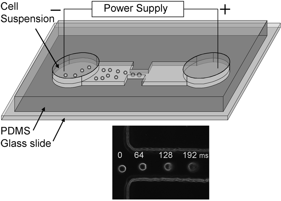
Schematic of a microfluidic electroporative flow cytometer
Download image
caption below

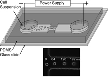
The research technique uses an electrical field within a microscopic fluid-filled channel through which a cell moves. As the cell is exposed to the electricity, it swells.

The cell expansion results because as cancer develops, it compromises the cell's structure, or cytoskeleton. A metastatic cancer cell cytoskeleton is more prone to deformity than a primary cancer cell or a normal cell, said Lu, an assistant professor of agricultural and biological engineering. When cells were put through the electrical field that Lu and his colleagues used, pores opened in the cell membrane, allowing fluid from the microchannel into the cell itself.

Just like a person gaining a lot of weight, the cells balloon in size, with the biggest deformity appearing in the metastatic cells.

"Our approach - microfluidic electroporative flow cytometry - can exactly characterize the degree to which a cell can become deformed," Lu said.

A patent is pending on the technique.

The amount of electricity and the length of time the cell is exposed to it also determined how much the various types of cells expanded. Under the parameters that Lu's team used, the metastatic cells expanded by 75 percent after electroporation, while primary cancer cells and normal cells expanded by 50 percent and 25 percent, respectively.

The Purdue scientists used a camera to measure how many cells were being screened over a predetermined time period. The camera must be able to capture changes in each cell one frame at a time.

The scientists want to make the screening process even faster, so they need a camera that can shoot frames even more rapidly than the one Lu's team used for this study. This would provide more accurate measurement of cell expansion. They also want to use the technique to diagnose other types of cancers and other diseases. Tests on a blood disease already are under way.

The eventual goal is to apply microfluidic electroporative flow cytometry in patient trials, Lu said.

"But things become more complicated if you're dealing with patient tissues rather than cell lines," he said. "Cell lines contain only one type of cell; patient tissues have different kinds of cells."

The Wallace H. Coulter Foundation and the National Science Foundation funded this study.

Lu also has appointments in Purdue's Weldon School of Biomedical Engineering, School of Chemical Engineering and the Laboratory for Renewable Resources Engineering. Department of Agricultural and Biological Engineering postdoctoral student Ning Bao and graduate student Yihong Zhan co-authored the paper.

Writer: Susan A. Steeves, (765) 496-7481, ssteeves@purdue.edu

Source: Chang Lu, (765) 494-1188, changlu@purdue.edu

Ag Communications: (765) 494-2722;
Beth Forbes, forbes@purdue.edu
Agriculture News Page

IMAGE CAPTION:
This schematic shows a microfluidic electroporative flow cytometer. The inset image shows the continuous increase in the cell size as the cell flows in the electrical field. (Purdue University graphic)


ABSTRACT

Microfluidic Electroporative Flow Cytometry for Studying Single Cell Biomechanics

Ning Bao, Yihong Zhan, Chang Lu - Department of Agricultural and Biological Engineering, Weldon School of Biomedical Engineering, School of Chemical Engineering, Purdue University, West Lafayette, IN 47907

Biomechanical properties of cells yield important information on the disease state of cells, such as transformation and metastasis. Screening of cells based on their biomechanical properties provides rapid tools for label-free diagnosis and staging of cancers. However, existent single cell techniques for measuring biomechanical properties suffer from low throughput (min). This prevents the application of these assays to a large cell population, which produces information with statistical significance. In this study, we applied microfluidics-based electroporative flow cytometry (EFC) that combined electroporation with flow cytometry to study deformability of cells at the single cell level with a throughput of ~5 cells/s. The cell swelling during flow-through electroporation was recorded in real time. We believe that the degree of such swelling was indicative of the cell deformability and the cytoskeleton mechanics. Three cell types (MCF-10A, MCF-7 and 12-O-tetradecanoylphorbol-13-acetate (TPA) treated MCF-7) with different malignancy and metastatic potential were tested using our approach. We found that the more malignant and metastatic cell types exhibited more swelling due to higher cell deformability. Furthermore, the disruption of microtubules by colchicine caused substantial change in the EFC results, which confirmed that EFC data strongly reflected the cytoskeletal mechanics. Finally, the cell type with the highest metastatic potential also suffered the most cell death due to the flow-through electroporation treatment, presumably due to the most substantial cell swelling which could irreversibly rupture the membrane. EFC provides a new method for examining single cell biomechanics with high throughput. We believe that this technique will be useful for mechanistic studies of cytoskeleton dynamics and clinical applications such as diagnosis and staging of cancers in general.

Source

Ref:

National Science Foundation awards prestigious grant to Purdue researcher

Publication Date: 11/14/2008

Anal. Chem., 80 (20), 77147719, 2008. 10.1021/ac801060t

Web Release Date: September 18, 2008

Copyright © 2008 American Chemical Society

Microfluidic Electroporative Flow Cytometry for Studying Single-Cell Biomechanics

Ning Bao, Yihong Zhan, and Chang Lu*

Department of Agricultural and Biological Engineering, Weldon School of Biomedical Engineering, School of Chemical Engineering, Purdue University, West Lafayette, Indiana 47907

Thursday, November 13, 2008

A metal-free polymeric photocatalyst for hydrogen production from water under visible light

Article abstract

Nature Materials

Published online: 9 November 2008 | doi:10.1038/nmat2317

A metal-free polymeric photocatalyst for hydrogen production from water under visible light

Xinchen Wang1,2, Kazuhiko Maeda3, Arne Thomas1, Kazuhiro Takanabe3, Gang Xin3, Johan M. Carlsson4, Kazunari Domen3 & Markus Antonietti1


Abstract

The production of hydrogen from water using a catalyst and solar energy is an ideal future energy source, independent of fossil reserves. For an economical use of water and solar energy, catalysts that are sufficiently efficient, stable, inexpensive and capable of harvesting light are required. Here, we show that an abundant material, polymeric carbon nitride, can produce hydrogen from water under visible-light irradiation in the presence of a sacrificial donor. Contrary to other conducting polymer semiconductors, carbon nitride is chemically and thermally stable and does not rely on complicated device manufacturing. The results represent an important first step towards photosynthesis in general where artificial conjugated polymer semiconductors can be used as energy transducers.

Max-Planck Institute of Colloids and Interfaces, Department of Colloid Chemistry, Research Campus Golm, 14424 Postdam, Germany
  1. Research Institute of Photocatalysis, State Key Laboratory Breeding Base of Photocatalysis, Fuzhou University, Fuzhou 350002, China
  2. Department of Chemical System Engineering, School of Engineering, The University of Tokyo, Bunkyo-ku, Tokyo 113-8656, Japan
  3. Fritz-Haber-Institute of the Max-Planck-Society, Theory Department, Faradayweg 4-6, D-14195 Berlin, Germany

Correspondence to: Xinchen Wang1,2 e-mail: xcwang@fzu.edu.cn

Correspondence to: Kazunari Domen3 e-mail: domen@chemsys.t.u-tokyo.ac.jp

Source

Wednesday, November 12, 2008

University embarks on carbon nanotube data storage project, promises DRAM-like non-volatile memory

Trendwatch
By Rick C. Hodgin
Wednesday, November 12, 2008 03:30

Nottingham (UK) - Researchers at The University of Nottingham, one of UK's Top 10 universities, also ranking in the world's Top 100, stated yesterday that Project Nanodevice is underway. Their goal is to create molecular memory built of telescoping carbon nanotubes. "In this project a new device for storing information will be developed, made entirely of carbon nanotubes and combining the speed and price of dynamic memory with the non-volatility of flash memory."


Telescoping a carbon nanotube

The idea sounds simple enough; two carbon nanotubes of slightly different size, one resting inside the other like a two-member set of matryoshka (Russian dolls where each one has a smaller one inside). Electrical current will pass through the outer tube forcing the inner tube to telescope in or out. When out it will make contact with a remote electrode, thereby completing a circuit to create a binary one. When retracted the circuit will be broken - a binary zero.


Image
An artist's rendition of carbon nanotube memory in theory. (a) shows a full extended telescope and completed circuit representing a binary one. (b) shows a retracted telescope and an incomplete circuit creating a binary zero. Single-atom thick walls allow massive storage potential on the order of 10-100x more dense than modern flash memory with read/write speeds rivaling DRAM.


This kind of memory will be a physical displacement of matter, meaning something has to move in order to switch states. Tiny, rolled sheets of graphene make up the carbon nanotubes, and these exhibit molecular properties which make the movements extremely fast and reliable, at least theoretically.


Non-volatile, fast and friendly

Another advantage of this system is that the memory will be non-volatile. Just like flash memory today, it won't need any power to maintain its state. It should also be extremely resistant to G-force induced state changes, such as accidental droppage.

Even early generations of this technology should be as fast or faster than modern DRAM. Future computers using this kind of memory won't have a separate memory and hard disk for storage. Theirs will be a unified memory architecture built around this kind of storage medium, a new design paradigm for the instant on computer, one capable of continuous processing and data storage without ever swapping memory out to hard disk through paging. This one fact alone would greatly speed up our computer experience today.


"Project"ions

The project is being led by Dr. Elena Bichoutskaia, who said, "The electronics industry is searching for a replacement of silicon-based technologies for data storage and computer memory. Existing technologies, such as magnetic hard discs, cannot be used reliably at the sub-micrometre scale and will soon reach their fundamental physical limitations."

Her goals, and the goals of the research teams working on this project, is a new memory device. According to Bichoutskaia, a new carbon nanotube memory product will be produced, one that will replacing DRAM and flash. With research of this nature there are no timeframes.

Personally, I suggest a name for this creation, one in keeping with the finest traditions of existing memory naming conventions: CRAM (Carbon-nanotube RAM). "How many smaller nanotubes can I cram inside the bigger ones?" Perhaps future generations could move away from binary computers into ternary (or beyond) by having multiple tubes, like a real telescope.

Source

Tuesday, November 11, 2008

Drill, baby, drill - with nanotechnology

Posted: November 11, 2008
(Nanowerk Spotlight) As we have show before, nanotechnology applications could provide decisive technological breakthroughs in the energy sector and have a considerable impact on creating the sustainable energy supply that is required to make the transition from fossil fuels. Although we love to write about all the clean and green applications that will be nanotechnology enabled, the harsh reality is that dirty energy is still fuelling our way of life.
No matter if you are a member of the "drill, baby, drill" crowd or if you are actively involved in saving energy and think that the development of renewable energies can't come fast enough, we have to live with the fact that the world's energy production will continue to depend on oil, gas and coal for quite a few more years. But even here, nanotechnology applications might offer some improvements.
A new report shows that nanotechnology, in the form of carbon nanotube (CNT) rubber composites, could help to significantly enhance oil production efficiency by allowing to probe and drill deeper wells. This in turn might allow to better exploit existing oil fields and maybe weaken the argument for new drilling in environmentally sensitive areas.
While there is a hot debate going on if the world is close to, or already has reached, "peak oil" – the time when global oil production begins a terminal decline – oil companies today are faced with increased production difficulties. The problem is that the oil and gas industry has already picked much of the low-hanging fruit when it comes to exploring oil reservoirs. Much of the remaining oil resources will increasingly have to be produced from more difficult to recover residuals – primary recovery can typically extract only 10% to 30% of the oil in place – and in deeper and less accessible reservoirs. If you are interested to learn more, the International Energy Agency has produced a publication ("Resources to Reserves" - pdf download, 4.7 MB) that identifies challenges and key technologies being investigated in the exploration, production and transportation of oil and gas.
Downhaul devices in underground resources probing use rubber seals as a key component
Downhaul devices in underground resources probing use rubber seals as a key component. (Reprinted with permission from Wiley)
Some of the technical challenges in recovering untapped oil resources have to do with the extreme heat and pressure that oil drilling equipment is exposed to when certain depths are reached. One of the materials that is being stretched to its limits in extreme conditions is rubber. Rubbers are almost exclusively used as a sealing material in oil probing and excavation, typically as O-rings and sealants between the various joining modules of a drill or probe.
Modern rubbers' performance limits are typically reached when temperatures exceed 200°C or pressures go beyond 200 MPa and commonly used O-rings in oil exploration operate under typical temperatures and pressures such as 175°C and 135 MPa. Formulating rubber that has the ability to withstand higher temperatures and pressures has been a serious technological challenge in oil & gas exploration.
"Generally, carbon black-filled fluorine rubber has been used as a sealant in oil exploration to date" Dr. Morinobu Endo explains to Nanowerk. "Although several papers regarding carbon nanotube-filled rubber composites have been published, no one – to the best of our knowledge – has found a way to significantly improve the heat resistance and durability of carbon nanotube/rubber composites. This has been due to the great difficulty of dispersing carbon nanotubes homogeneously, and the lack of strong binding interactions between the filler and the rubber matrix."
In order to accomplish the homogeneous dispersion of carbon nanotubes within the matrix rubber, Endo and an international team of collaborators developed a milling process at low temperature to get enhanced elasticity and shear force. The result is an extreme-performance rubber nanocomposite material that is able to withstand temperatures of up to 260°C and pressures as high as 239 MPa.
"Based on our team's estimate by surveying the depths and temperatures of oil resources, the development of an extreme rubber sealant having the enhanced performance of 100°C higher temperature and 70 MPa higher pressure durability, as compared to those of the currently used O-rings, will contribute to doubling the current average oil recovery efficiency by incorporation with other related technological innovations" says Endo.
The distribution of temperature and pressure of some current oil wells
The distribution of temperature and pressure of some current oil wells. The new rubber nanocomposite will allow excavating oil from unreachable deposits found deeper and at higher temperatures (as high as 260°C at 239 MPa). The authors would like to thank Dr. T. Baird for his permission to use his original figure in High-Pressure, high-temperature well logging, perforating and testing (pdf download, 633 KB). The high ability to withstand at high temperature and high pressure enables the extractable oil to be twice compared to the current technology. (Graphic: Dr. Endo)
Endo, a Professor of Electrical & Electronic Engineering at Shinshu University in Japan, collaborated with professors Kenji Takeuchi, Takuya Hayashi, and Yoong Ahm Kim from his university as well as Mauricio Terrones from IPICYT in Mexico, Mildred Dresselhaus at MIT, and scientists from Nissin Kogyo, Schlumberger, and Fukoko. The team published their findings in the October 21, 2008 online edition of Advanced Functional Materials ("Extreme-Performance Rubber Nanocomposites for Probing and Excavating Deep Oil Resources Using Multi-Walled Carbon Nanotubes").
The scientists point out that the use of their novel CNT/rubber nanocomposite material is not limited to oil exploration but could be suitable for a wide range of innovative applications ranging from factory tools to environmental applications to aerospace and space technologies.
To develop their rubber nanocomposite, the researchers used a low-temperature roll mill process to disperse multi-walled carbon nanotubes in a synthetic rubber matrix (Fluoroelastomers/FKM). Endo explains that the three key issues in making the nanocomposite are the use of of multi-walled carbon nanotubes embedded in fluorinated rubber, the surface modification of these nanotubes, and the formation of a cellulation structure in the composite.
In order to accomplish the homogeneous dispersion of carbon nanotubes within the matrix rubber, the team developed a milling process at low-temperature to get enhanced elasticity and shear force, where the temperature of the roll mill was maintained at less than 20"C. Endo explains that this process allows three important things: "1) the elastomer molecules of the matrix to fill the voids created by the physically intermingled nanotubes, thus breaking effectively their intrinsic agglomeration during the mixing process, 2) the rubber matrix to exhibit good wettability with carbon nanotubes, and 3) the rubber matrix to display extreme elasticity."
To demonstrate an innovative end-use based of the their novel nanocomposite, Endo and his collaborators developed a rubber sealant for oil exploration and probing purposes, which is applicable under extremely harsh conditions. Testing their nanocomposite O-rings, they found that they exhibited higher pressure-resistant properties when compared to conventional sealants by about 80–100 MPa higher pressure, which corresponds to a much deeper depth in water of 8000 meters.
"Our experimental system was limited in its ability to simulate further extreme conditions, but we believe that our new rubber composite may actually exceed our claims" says Endo. He cautions, though, that they have not yet developed an effective mass-production technique for this CNT/rubber nanocomposite, so practical applications may have to wait a while.

By Michael Berger. Copyright 2008 Nanowerk LLC

Source

Report: Samsung SDI Investigating the Use of CNT in BLUs (July 16)

Industry officials revealed that Samsung SDI is in the process of considering carbon nanotube (CNT) material for use in its backlight unit (BLU) business, Display Bank reported on July 8.

Display Bank cited industry sources as stating that Samsung SDI has completed development of next-generation CNT BLU, which would emerge as the next technology in backlighting applications, after CCFL and LED. The company is exploring using the technology in various electronic products including LCD TVs larger than 40 inches.

According to Display Bank, CNT BLU could measure less than 1cm thick, and would offer benefits of both CCFL and LED BLU. A Samsung SDI-related spokesperson confirmed the "ongoing research of CNT BLU" to Display Bank but would not offer any specifics.

Source

Friday, November 7, 2008

SELF-ASSEMBLING AMPHIPHILIC POLYMERS AS ANTIVIRAL AGENTS

Title of Invention: SELF-ASSEMBLING AMPHIPHILIC POLYMERS AS ANTIVIRAL AGENTS

(Click pic for a clearer view)

International Application No.: PCT/US2007/001607
International Filing Date: 22.01.2007
Pub. No.: WO 2008/091246
WIPO Publication Date: 31.07.2008


USPTO Details:

PCT/US07/01607 SELF-ASSEMBLING AMPHIPHILIC POLYMERS AS ANTIVIRAL AGENTS Printer Friendly Version
Select New Case Application Data Transaction History Image File Wrapper Continuity Data Published Documents Correspondence Data Supplemental Content
Bibliographic Data
Application Number: PCT/US07/01607 Customer Number: -
Int'l. Filing Date: 01-22-2007 Status: PCT - International Search Report Mailed to IB
Application Type: PCT Status Date: 11-23-2007
Examiner Name: - Location: What is a Location? -
Group Art Unit: - Location Date: -
Confirmation Number: 3778 WIPO Publication No.: WO 2008/091246
Attorney Docket Number: 7609-02WO WIPO Publication Date: 07-31-2008
Class / Subclass: 001/PCT.007 Patent Number: -
First Named Inventor: - Issue Date of Patent: -

Link to USPTO

In the EPO:

SELF-ASSEMBLING AMPHIPHILIC POLYMERS AS ANTIVIRAL AGENTS


Bibliographic data

Description

Claims

Mosaics

Original document

INPADOC legal status

Publication number: WO2008091246 (A1)
Publication date: 2008-07-31
Inventor(s): ONTON ANN LOUISE [US]; DIWAN ANIL [US]; TATAKE JAYANT G [US]
Applicant(s): ALLEXCEL INC [US]; ONTON ANN LOUISE [US]; DIWAN ANIL [US]; TATAKE JAYANT G [US]
Classification:
- international: A61K31/795; A61P31/14; A61P31/16; C07K7/06; C07K7/08; A61K31/74; A61P31/00; C07K7/00
- European: A61K31/795; C07K7/08A
Application number: WO2007US01607 20070122
Priority number(s): WO2007US01607 20070122


View INPADOC patent family
View list of citing documents

View document in the European Register

Cited documents:

WO9826662 (A1)

WO2006034081 (A2)

(To follow the progress to patent grant)


Abstract of WO 2008091246 (A1)
There are provided amphiphilic biodegradable copolymers comprising a hydrophilic backbone with pendant aliphatic groups as the hydrophobic component. The polymers form nanoscale molecular aggregates in aqueous environments, which have hydrophobic interiors that are capable of solubilizing insoluble organic compounds and disrupting viral coat proteins. The polymers optionally feature reactive functional groups that provide attachment points for antibodies, ligands, and other targeting moieties which mediate adherence of the aggregate to a viral target.
EPO Souce

Company: NanoViricides (NNVC)