Showing posts with label QDs. Show all posts

Monday, February 21, 2011

Researchers fabricate first large-area, full-color quantum dot display

February 21, 2011 by Lisa Zyga

quantum dot display

Enlarge

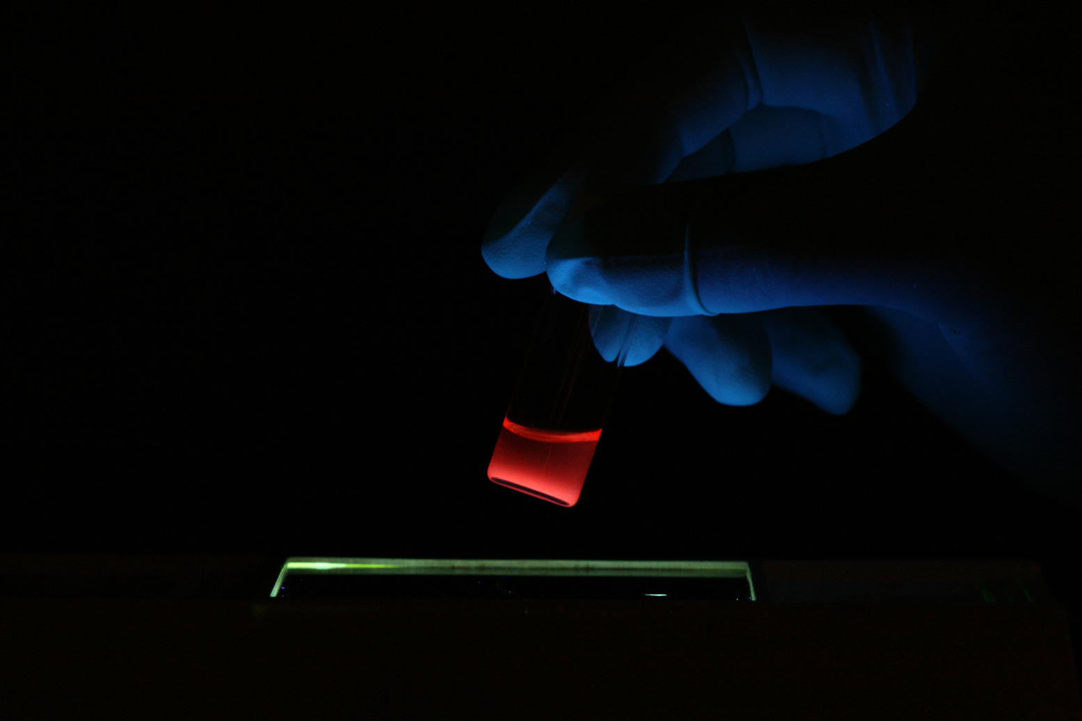
Electroluminescence image of a four-inch full-color quantum dot display with a resolution of 320 x 240 pixels. Image credit: Tae-Ho Kim, et al. ©2011 Macmillan Publishers Limited.

(PhysOrg.com) -- For more than a decade, researchers have been trying to make TV displays out of quantum dots. Theoretically, quantum dot displays could provide extremely high-resolution images and higher energy efficiencies than current TVs. Now in a new study, researchers have presented the first large-area, full-color quantum dot display that could lead to the development of displays for the next-generation TVs, mobile phones, digital cameras, and portable game systems.

The researchers, Tae-Ho Kim and coauthors from various institutes in South Korea, have published their study on the first four-inch, full-color quantum dot display in a recent issue of Nature Photonics. The display consists of a film printed with trillions of the tiny (an average of 3 trillion per cm2). The quantum dots emit light at a specific wavelength (color) that can be tuned by changing the size of the quantum dots.

Previous attempts to make full-color quantum dot displays have faced challenges in that image quality tended to decrease with the size of the display. To overcome this challenge, the researchers in the current study used a different method for applying the quantum dots to the film’s surface. Instead of spraying the quantum dots onto the film, the researchers created an “ink stamp” out of a patterned silicon wafer. They used the stamp to pick up strips of size-selected quantum dots, and then stamp them onto the substrate. Unlike the spraying methods, this method does not require the use of a solvent, which previously reduced color brightness.

As the results showed, the new quantum dot display has a greater density and uniformity of quantum dots, as well as a brighter picture and higher energy efficiency than previous quantum dot displays. The new display is also flexible, so applications could include roll-up portable displays or flexible lighting applications. The technology could also be used in photovoltaic devices, which would especially benefit from quantum dots’ high energy efficiency.

More information: Tae-Ho Kim, et al. “Full-colour quantum dot displays fabricated by transfer printing.” Nature Photonics. DOI:10.1038/nphoton.2011.12.
via: Nature News

Source

Sunday, February 20, 2011

Researchers develop new technology for cheaper, more efficient solar cells

Posted: Feb 20th, 2011
(Nanowerk News) The sun provides more than enough energy for all our needs, if only we could harness it cheaply and efficiently. Solar energy could provide a clean alternative to fossil fuels, but the high cost of solar cells has been a major barrier to their widespread use.
Stanford researchers have found that adding a single layer of organic molecules to a solar cell can increase its efficiency three-fold and could lead to cheaper, more efficient solar panels. Their results were published online in ACS Nano on Feb. 7.
Professor of chemical engineering Stacey Bent first became interested in a new kind of solar technology two years ago. These solar cells used tiny particles of semiconductors called "quantum dots." Quantum dot solar cells are cheaper to produce than traditional ones, as they can be made using simple chemical reactions. But despite their promise, they lagged well behind existing solar cells in efficiency.
"I wondered if we could use our knowledge of chemistry to improve their efficiency," Bent said. If she could do that, the reduced cost of these solar cells could lead to mass adoption of the technology.
Bent will discuss her research on Sunday, Feb. 20, at 8:30 a.m. Eastern, at the annual meeting of the American Association for the Advancement of Science in Washington, D.C.
In principle, quantum dot cells can reach much higher efficiency, Bent said, because of a fundamental limitation of traditional solar cells.
Solar cells work by using energy from the sun to excite electrons. The excited electrons jump from a lower energy level to a higher one, leaving behind a "hole" where the electron used to be. Solar cells use a semiconductor to pull an electron in one direction, and another material to pull the hole in the other direction. This flow of electron and hole in different directions leads to an electric current.
But it takes a certain minimum energy to fully separate the electron and the hole. The amount of energy required is specific to different materials and affects what color, or wavelength, of light the material best absorbs. Silicon is commonly used to make solar cells because the energy required to excite its electrons corresponds closely to the wavelength of visible light.
But solar cells made of a single material have a maximum efficiency of about 31 percent, a limitation of the fixed energy level they can absorb.
Quantum dot solar cells do not share this limitation and can in theory be far more efficient. The energy levels of electrons in quantum dot semiconductors depends on their size – the smaller the quantum dot, the larger the energy needed to excite electrons to the next level.
So quantum dots can be tuned to absorb a certain wavelength of light just by changing their size. And they can be used to build more complex solar cells that have more than one size of quantum dot, allowing them to absorb multiple wavelengths of light.
Because of these advantages, Bent and her students have been investigating ways to improve the efficiency of quantum dot solar cells, along with associate Professor Michael McGehee of the department of Materials Science and Engineering.
The researchers coated a titanium dioxide semiconductor in their quantum dot solar cell with a very thin single layer of organic molecules. These molecules were self-assembling, meaning that their interactions caused them to pack together in an ordered way. The quantum dots were present at the interface of this organic layer and the semiconductor. Bent's students tried several different organic molecules in an attempt to learn which ones would most increase the efficiency of the solar cells.
But she found that the exact molecule didn't matter – just having a single organic layer less than a nanometer thick was enough to triple the efficiency of the solar cells. "We were surprised, we thought it would be very sensitive to what we put down," said Bent.
But she said the result made sense in hindsight, and the researchers came up with a new model – it's the length of the molecule, and not its exact nature, that matters. Molecules that are too long don't allow the quantum dots to interact well with the semiconductor.
Bent's theory is that once the sun's energy creates an electron and a hole, the thin organic layer helps keep them apart, preventing them from recombining and being wasted. The group has yet to optimize the solar cells, and they have currently achieved an efficiency of, at most, 0.4 percent. But the group can tune several aspects of the cell, and once they do, the three-fold increase caused by the organic layer would be even more significant.
Bent said the cadmium sulfide quantum dots she is currently using are not ideal for solar cells, and the group will try different materials. She said she would also try other molecules for the organic layer, and could change the design of the solar cell to try to absorb more light and produce more electrical charge. Once Bent has found a way to increase the efficiency of quantum dot solar cells, she said she hopes their lower cost will lead to wider acceptance of solar energy.
Source: Stanford University

Source


Article [Source URL]

Effects of Self-Assembled Monolayers on Solid-State CdS Quantum Dot Sensitized Solar Cells
Pendar Ardalan, Thomas P. Brennan, Han-Bo-Ram Lee, Jonathan R. Bakke, I-Kang Ding, Michael D. McGehee, and Stacey F. Bent*
Department of Chemical Engineering
Department of Materials Science and Engineering
Stanford University, Stanford, California 94305, United States
ACS Nano, Article ASAP
DOI: 10.1021/nn103371v
Publication Date (Web): February 7, 2011
Copyright © 2011 American Chemical Society
*Address correspondence to sbent@stanford.edu.

Abstract

Abstract Image

Quantum dot sensitized solar cells (QDSSCs) are of interest for solar energy conversion because of their tunable band gap and promise of stable, low-cost performance. We have investigated the effects of self-assembled monolayers (SAMs) with phosphonic acid headgroups on the bonding and performance of cadmium sulfide (CdS) solid-state QDSSCs. CdS quantum dots 2 to 6 nm in diameter were grown on SAM-passivated planar or nanostructured TiO2 surfaces by successive ionic layer adsorption and reaction (SILAR), and photovoltaic devices were fabricated with spiro-OMeTAD as the solid-state hole conductor. X-ray photoelectron spectroscopy, Auger electron spectroscopy, ultraviolet−visible spectroscopy, scanning electron microscopy, transmission electron microscopy, water contact angle measurements, ellipsometry, and electrical measurements were employed to characterize the materials and the resulting device performance. The data indicate that the nature of the SAM tailgroup does not significantly affect the uptake of CdS quantum dots on TiO2 nor their optical properties, but the presence of the SAM does have a significant effect on the photovoltaic device performance. Interestingly, we observe up to 3 times higher power conversion efficiencies in devices with a SAM compared to those without the SAM.

Keywords ():

quantum dot sensitized solar cells; self-assembled monolayers; successive ionic layer adsorption and reaction; cadmium sulfide; titanium dioxide; nanostructure

Friday, November 20, 2009

Turning heat to electricity

David L. Chandler, MIT News Office

MIT research points to a much more efficient way of harvesting electrical power from what would otherwise be wasted heat.

In everything from computer processor chips to car engines to electric powerplants, the need to get rid of excess heat creates a major source of inefficiency. But new research points the way to a technology that might make it possible to harvest much of that wasted heat and turn it into usable electricity.

That kind of waste-energy harvesting might, for example, lead to cellphones with double the talk time, laptop computers that can operate twice as long before needing to be plugged in, or power plants that put out more electricity for a given amount of fuel, says Peter Hagelstein, co-author of a paper on the new concept appearing this month in the Journal of Applied Physics.

Hagelstein, an associate professor of electrical engineering at MIT, says existing solid-state devices to convert heat into electricity are not very efficient. The new research, carried out with graduate student Dennis Wu as part of his doctoral thesis, aimed to find how close realistic technology could come to achieving the theoretical limits for the efficiency of such conversion.

Theory says that such energy conversion can never exceed a specific value called the Carnot Limit, based on a 19th-century formula for determining the maximum efficiency that any device can achieve in converting heat into work. But current commercial thermoelectric devices only achieve about one-tenth of that limit, Hagelstein says. In experiments involving a different new technology, thermal diodes, Hagelstein worked with Yan Kucherov, now a consultant for the Naval Research Laboratory, and coworkers to demonstrate efficiency as high as 40 percent of the Carnot Limit. Moreover, the calculations show that this new kind of system could ultimately reach as much as 90 percent of that ceiling.

Hagelstein, Wu and others started from scratch rather than trying to improve the performance of existing devices. They carried out their analysis using a very simple system in which power was generated by a single quantum-dot device — a type of semiconductor in which the electrons and holes, which carry the electrical charges in the device, are very tightly confined in all three dimensions. By controlling all aspects of the device, they hoped to better understand how to design the ideal thermal-to-electric converter.

Hagelstein says that with present systems it’s possible to efficiently convert heat into electricity, but with very little power. It’s also possible to get plenty of electrical power — what is known as high-throughput power — from a less efficient, and therefore larger and more expensive system. “It’s a tradeoff. You either get high efficiency or high throughput,” says Hagelstein. But the team found that using their new system, it would be possible to get both at once, he says.

A key to the improved throughput was reducing the separation between the hot surface and the conversion device. A recent paper by MIT professor Gang Chen reported on an analysis showing that heat transfer could take place between very closely spaced surfaces at a rate that is orders of magnitude higher than predicted by theory. The new report takes that finding a step further, showing how the heat can not only be transferred, but converted into electricity so that it can be harnessed.

A company called MTPV Corp. (for Micron-gap Thermal Photo-Voltaics), founded by Robert DiMatteo SM ’96, MBA ‘06, is already working on the development of “a new technology closely related to the work described in this paper,” Hagelstein says.

DiMatteo says he hopes eventually to commercialize Hagelstein’s new idea. In the meantime, he says the technology now being developed by his company, which he expects to have on the market next year, could produce a tenfold improvement in throughput power over existing photovoltaic devices, while the further advance described in this new paper could make an additional tenfold or greater improvement possible. The work described in this paper “is potentially a major finding,” he says.

DiMatteo says that worldwide, about 60 percent of all the energy produced by burning fuels or generated in powerplants is wasted, mostly as excess heat, and that this technology could “make it possible to reclaim a significant fraction of that wasted energy.”

When this work began around 2002, Hagelstein says, such devices “clearly could not be built. We started this as purely a theoretical exercise.” But developments since then have brought it much closer to reality.

While it may take a few years for the necessary technology for building affordable quantum-dot devices to reach commercialization, Hagelstein says, “there’s no reason, in principle, you couldn’t get another order of magnitude or more” improvement in throughput power, as well as an improvement in efficiency.

“There’s a gold mine in waste heat, if you could convert it,” he says. The first applications are likely to be in high-value systems such as computer chips, he says, but ultimately it could be useful in a wide variety of applications, including cars, planes and boats. “A lot of heat is generated to go places, and a lot is lost. If you could recover that, your transportation technology is going to work better.”


United States Patent7,390,962
Greiff , et al.June 24, 2008

Micron gap thermal photovoltaic device and method of making the same

Abstract

A method of making a micron gap thermal photovoltaic device wherein at least one standoff is formed on a photovoltaic substrate, a sacrificial layer is deposited on the photovoltaic substrate and about the standoff, an emitter is attached to the standoff and has a lower planar surface separated from the photovoltaic substrate by the sacrificial layer, and the sacrificial layer is removed to form a sub-micron gap between the photovoltaic substrate and the lower planar surface of the emitter.


Inventors:Greiff; Paul (Wayland, MA), DiMatteo; Robert Stephen (Belmont, MA)
Assignee:The Charles Stark Draper Laboratory, Inc. (Cambridge, MA)
Appl. No.:10/443,414
Filed:May 22, 2003

Source

Tuesday, September 16, 2008

Researchers Develop Nano-Sized ‘Cargo Ships’ to Target and Destroy Tumors

September 11, 2008

By Kim McDonald

Scientists have developed nanometer-sized ‘cargo ships’ that can sail throughout the body via the bloodstream without immediate detection from the body’s immune radar system and ferry their cargo of anti-cancer drugs and markers into tumors that might otherwise go untreated or undetected.

Photo of Ji-Ho Park holding a vial containing the nanometer-sized cargo ships
UCSD graduate student Ji-Ho Park holds a vial containing the nanometer-sized cargo ships, composed of a magnetic nanoparticle, a fluorescent quantum dot and an anti-cancer drug molecule that will be left on the site of the tumor.

Credit: Luo Gu, UCSD

In a forthcoming issue of the Germany-based chemistry journal Angewandte Chemie, scientists at UC San Diego, UC Santa Barbara and MIT report that their nano-cargo-ship system integrates therapeutic and diagnostic functions into a single device that avoids rapid removal by the body’s natural immune system. Their paper is now accessible in an early online version here.

“The idea involves encapsulating imaging agents and drugs into a protective ‘mother ship’ that evades the natural processes that normally would remove these payloads if they were unprotected,” said Michael Sailor, a professor of chemistry and biochemistry at UCSD who headed the team of chemists, biologists and engineers that turned the fanciful concept into reality. “These mother ships are only 50 nanometers in diameter, or 1,000 times smaller than the diameter of a human hair, and are equipped with an array of molecules on their surfaces that enable them to find and penetrate tumor cells in the body.”

These microscopic cargo ships could one day provide the means to more effectively deliver toxic anti-cancer drugs to tumors in high concentrations without negatively impacting other parts of the body.

“Many drugs look promising in the laboratory, but fail in humans because they do not reach the diseased tissue in time or at concentrations high enough to be effective,” said Sangeeta Bhatia, a physician, bioengineer and professor of Health Sciences and Technology at MIT who played a key role in the development. “These drugs don’t have the capability to avoid the body’s natural defenses or to discriminate their intended targets from healthy tissues. In addition, we lack the tools to detect diseases such as cancer at the earliest stages of development, when therapies can be most effective.”

The researchers designed the hull of the ships to evade detection by constructing them of specially modified lipids--a primary component of the surface of natural cells. The lipids were modified in such a way as to enable them to circulate in the bloodstream for many hours before being eliminated. This was demonstrated by the researchers in a series of experiments with mice.

The researchers also designed the material of the hull to be strong enough to prevent accidental release of its cargo while circulating through the bloodstream. Tethered to the surface of the hull is a protein called F3, a molecule that sticks to cancer cells. Prepared in the laboratory of Erkki Ruoslahti, a cell biologist and professor at the Burnham Institute for Medical Research at UC Santa Barbara, F3 was engineered to specifically home in on tumor cell surfaces and then transport itself into their nuclei.

Photo of a vial of anti-cancer nano ships glows red under a black light.
A vial of anti-cancer nano ships glows red under a black light. The particles glow red because they contain fluorescent "quantum dot" nanoparticles.

Credit: Luo Gu, UCSD

“We are now constructing the next generation of smart tumor-targeting nanodevices,” said Ruoslahti. “We hope that these devices will improve the diagnostic imaging of cancer and allow pinpoint targeting of treatments into cancerous tumors.”

The researchers loaded their ships with three payloads before injecting them in the mice. Two types of nanoparticles, superparamagnetic iron oxide and fluorescent quantum dots, were placed in the ship’s cargo hold, along with the anti-cancer drug doxorubicin. The iron oxide nanoparticles allow the ships to show up in a Magnetic Resonance Imaging, or MRI, scan, while the quantum dots can be seen with another type of imaging tool, a fluorescence scanner.

“The fluorescence image provides higher resolution than MRI,” said Sailor. “One can imagine a surgeon identifying the specific location of a tumor in the body before surgery with an MRI scan, then using fluorescence imaging to find and remove all parts of the tumor during the operation.”

The team found to its surprise in its experiments that a single mother-ship can carry multiple iron oxide nanoparticles, which increases their brightness in the MRI image.

“The ability of these nanostructures to carry more than one superparamagnetic nanoparticle makes them easier to see by MRI, which should translate to earlier detection of smaller tumors,” said Sailor. “The fact that the ships can carry very dissimilar payloads—a magnetic nanoparticle, a fluorescent quantum dot, and a small molecule drug—was a real surprise.”

The researchers noted that the construction of so-called “hybrid nanosystems” that contain multiple different types of nanoparticles is being explored by several other research groups. While hybrids have been used for various laboratory applications outside of living systems, said Sailor, there are limited studies done in vivo, or within live organisms, particularly for cancer imaging and therapy.

“That’s because of the poor stability and short circulation times within the blood generally observed for these more complicated nanostructures,” he added. As a result, the latest study is unique in one important way.

Illustration of a vial of anti-cancer nano ships glows red under a black light.
The nanometer-sized cargo ships look individually like a chocolate-covered nut cluster, in which a biocompatible lipid forms the chocolate shell and magnetic nanoparticles, quantum dots and the drug doxorubicin are the nuts.

Credit: Ji-Ho Park, UCSD

“This study provides the first example of a single nanomaterial used for simultaneous drug delivery and multimode imaging of diseased tissue in a live animal,” said Ji-Ho Park, a graduate student in Sailor’s laboratory who was part of the team. Geoffrey von Maltzahn, a graduate student working in Bhatia’s laboratory, was also involved in the project, which was financed by a grant from the National Cancer Institute of the National Institutes of Health.

The nano mother ships look individually like a chocolate-covered nut cluster, in which a biocompatible lipid forms the chocolate shell and magnetic nanoparticles, quantum dots and the drug doxorubicin are the nuts. They sail through the bloodstream in groups that, under the electron microscope, look like small, broken strands of pearls.

The researchers are now working on developing ways to chemically treat the exteriors of the nano ships with specific chemical “zip codes,” that will allow them to be delivered to specific tumors, organs and other sites in the body.

Media Contact: Kim McDonald, 858-534-7572
Comment: Michael Sailor, 858-534-8188

Source

Tuesday, May 20, 2008

Titania–germanium nanocomposite for photo-thermo-electric application

Sukti Chatterjee 2008 Nanotechnology 19 265701 (9pp) doi: 10.1088/0957-4484/19/26/265701 Help

PDF (1.72 MB) | References


Sukti Chatterjee1
Center for Composite Materials, University of Delaware, Newark, DE 19716, USA
1 Present address: Naval Materials Research Laboratory, Defence Research and Development Organization, Ambernath e 421 506, India
E-mail: Sukti@yahoo.com

Abstract. The introduction of germanium (Ge) into titania (TiO2) creates an attractive semiconductor. The new semiconductor is named titania–germanium (TiO2–Ge). Ge dots are dispersed in the distorted TiO2 matrix of TiO2–Ge. The quantum Bohr radius of Ge is 24.3 nm, and hence the properties of the Ge dot can be varied by tailoring its size if it is smaller than its Bohr radius due to the quantum confinement effect (QCE). Therefore, simply by changing the Ge concentration, the morphology of TiO2–Ge can be varied within a wide range. Consequently, the optical, electronic and thermal properties of TiO2–Ge can be tailored. TiO2–Ge becomes a promising material for the next generation of photovoltaics as well as thermoelectric devices. It could also be used for photo-thermo-electric applications.

Print publication: Issue 26 (2 July 2008)
Received 14 December 2007, in final form 14 April 2008
Published 20 May 2008

PDF (1.72 MB) | References

Source